Oxide semiconductor, thin-film transistor and method for producing the same

a thin-film transistor and semiconductor technology, applied in semiconductor devices, inorganic chemistry, tin compounds, etc., can solve the problems of deterioration of materials, reduced efficiency, and relatively large power consumption of passive matrix types, so as to reduce the off current, improve the mobility, and keep the mobility

Inactive Publication Date: 2010-10-05
FUJI ELECTRIC CO LTD
View PDF6 Cites 59 Cited by
  • Summary
  • Abstract
  • Description
  • Claims
  • Application Information

AI Technical Summary

Benefits of technology

[0018]The present inventors have found that when Sn is added singly, Sn has a function of reducing the OFF current while keeping the mobility. Accordingly, it can be conceived that improvement of the mobility can be achieved while the OFF current is kept low when In and Sn are added simultaneously. Moreover, in the case of Zn, it can be conceived that when the same amount of Sn is added, SnZnO3 is formed as an amorphous material to thereby make it possible to improve the mobility while keeping the amorphous state. It can be also conceived that when the amount (x+1) of In and the amount (y+1) of Zn are added in predetermined ranges and the amount (z) of Sn is added together in a predetermined range close to x+y, the mobility is improved while the OFF current is kept low in an amorphous state. The condition concerned with x and y is 0≦x≦1 and −0.2≦y≦1.2, and the condition concerned with x, y and z is ⅓×(x+y)≦z≦2×(x+y). The last expression can be transformed to 0.5≦(x+y) / z≦3.
[0019]Accordingly, when oxide having an amorphous structure represented by general formula Inx+1MZny+1SnzO(4+1.5x+y+2z) (in which M=Ga or Al, 0≦x≦1, −0.2≦y≦1.2, z≧0.4, 0.5≦(x+y) / z≦3) is used as the oxide semiconductor, the carrier concentration can be reduced while the mobility is increased, although details of the mechanism thereof are unknown.
[0020]Accordingly, when the obtained amorphous oxide is further heat-treated under an oxidizing gas atmosphere, an oxide semiconductor having a low carrier concentration can be obtained stably. This can be conceived because structurally unstable portions are eliminated by heating as well as oxygen holes in the film are compensated by heat-treatment under the oxidizing atmosphere to thereby control the carrier concentration.
[0021]As described above, in accordance with the present invention, there can be provided an oxide semiconductor having an amorphous structure having higher mobility and capable of reducing a carrier concentration, a thin-film transistor, a method for producing the oxide semiconductor, and a method for producing the thin-film transistor.

Problems solved by technology

In comparison between the active matrix type drive method and the passive matrix drive method at the same display luminance, power consumption in the passive matrix type becomes relatively large because of reduction of this efficiency.
Moreover, increase of the current flowing in the organic EL element has a disadvantage that deterioration of material is apt to be caused by heating or the like and the life of the display unit is shortened.
However, the elongation of the light-emitting period lends itself to limitation of display capacity (number of drive lines) because the duty ratio for deciding the light-emitting time in the passive matrix type drive method is the reciprocal of the number of rows in the panel.
However, since polysilicon is a polycrystal, there is a large problem such that in-plane uniformity is poor particularly in a current drive type display such as an organic EL display.
Further, in amorphous silicon, in-plane uniformity is good because of the amorphous structure but there arises a problem that the mobility thereof is at most about 1 cm2 / Vs which is not enough to drive the organic EL element.

Method used


Image

  • Oxide semiconductor, thin-film transistor and method for producing the same
  • Oxide semiconductor, thin-film transistor and method for producing the same

Examples


examples 1 to 5

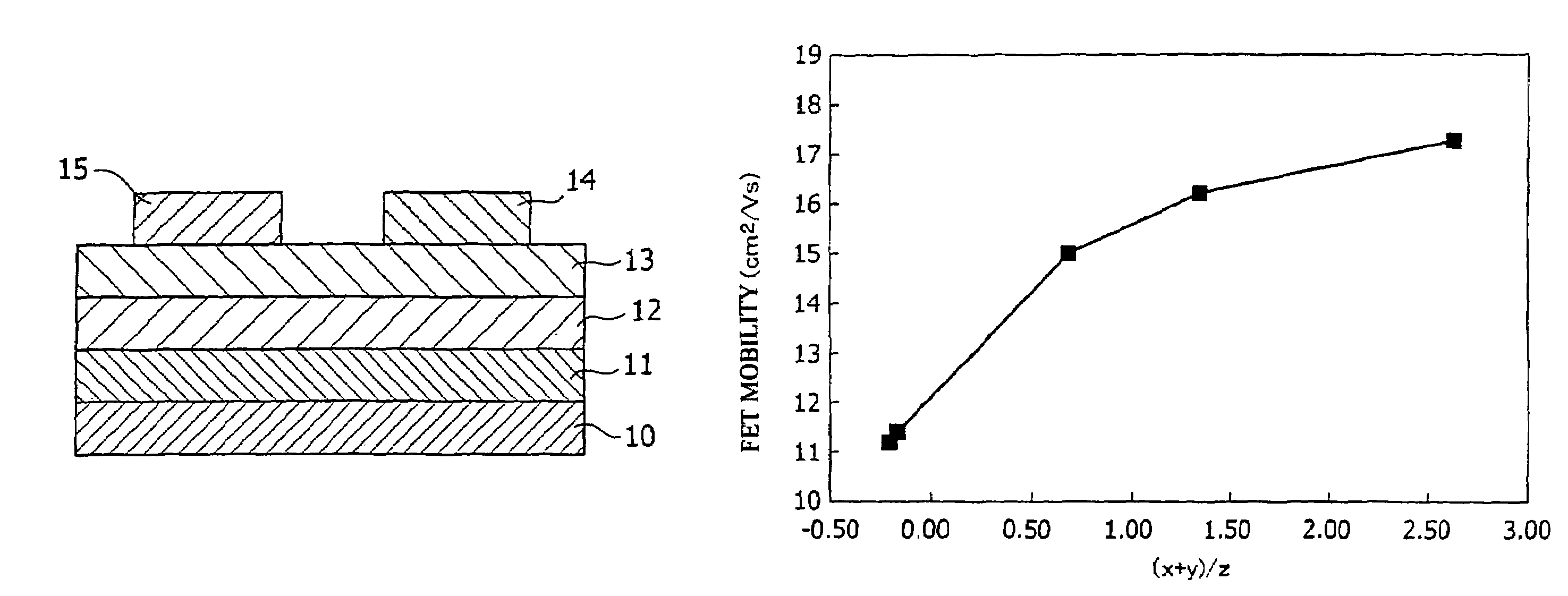
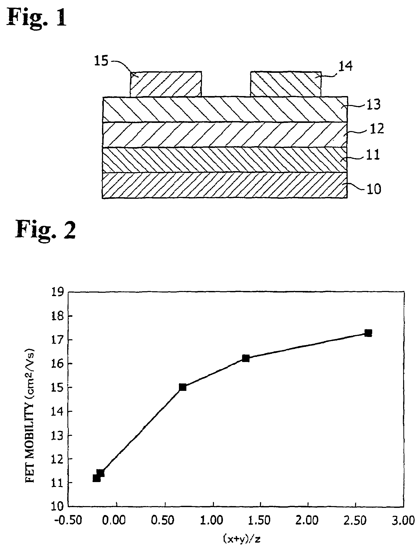
[0035]Five kinds of field-effect transistors each having the structure shown in FIG. 1 were produced as follows. First, a silicon wafer with a 100 nm-thick thermal oxide film was used as the substrate. The silicon wafer used was of a highly doped p-type and functioned as a gate electrode. The thermal oxide film functioned as a gate insulating film.

[0036]An oxide semiconductor was formed on the thermal oxide film by a high-frequency magnetron sputtering method. A pellet of metal oxide such as In2O3, ZnO or SnO2 with a small diameter was put on InGaZnO4 used as an oxide semiconductor target to thereby adjust the film composition. A condition that the substrate was not heated but put under an argon gas atmosphere at a vacuum of 2 Pa was used as the sputtering condition. The metal atom compositions of the thin films formed thus were evaluated by inductively coupled plasma optical emission spectrometric analysis (ICP). Each film composition as a result of the ICP was shown in Table 1. Th...


PUM


Abstract

Disclosed is an oxide semiconductor having an amorphous structure, wherein higher mobility and reduced carrier concentration are achieved. Also disclosed are a thin film transistor, a method for producing the oxide semiconductor, and a method for producing the thin film transistor. Specifically disclosed is an oxide semiconductor which is characterized by being composed of an amorphous oxide represented by the following a general formula: Inx+1MZny+1SnzO(4+1.5x+y+2z) (wherein M is Ga or Al, 0≦x≦1, −0.2≦y≦1.2, z≧0.4 and 0.5≦(x+y) / z≦3). This oxide semiconductor is preferably subjected to a heat treatment in an oxidizing gas atmosphere after film formation. Also specifically disclosed is a thin film transistor which is characterized by comprising the oxide semiconductor.

Description

RELATED APPLICATIONS[0001]The present application is based on International Application No. PCT / JP07 / 060686, filed on May 25, 2007, and claims priority from, Japanese Application Number 2006-144946, filed May 25, 2006, the disclosure of which is hereby incorporated by reference herein in its entirety.TECHNICAL FIELD[0002]The present invention relates to an oxide semiconductor, a thin-film transistor, a method for producing the oxide semiconductor, and a method for producing the thin-film transistor.BACKGROUND ART[0003]Flat displays for information apparatuses have become widespread remarkably in recent years. Among them, a liquid crystal display performs on / off control of light of a backlight unit by using the optical shuttering function of liquid crystal and obtains color by using color filters. On the contrary, an organic EL display (or an organic LED display) has not only an advantage such that the viewing angle is wide because each pixel emits light individually (that is, self-e...

Claims


Application Information

Patent Timeline
Patent Type & Authority Patents(United States)
IPC IPC(8): H01L21/00H01L21/84
CPCC01G19/006H01L29/78693H01L29/66969C01P2006/40
Inventor KATO, HISATOKAWAKAMI, HARUOSEKINE, NOBUYUKIKATO, KYOKO
Owner FUJI ELECTRIC CO LTD
Why Eureka
Try Eureka