Semiconductor laser element and method for producing same

a semiconductor and laser element technology, applied in semiconductor lasers, laser details, optical resonator shape and construction, etc., can solve the problems of inability to achieve the required characteristics for each use, inability to guarantee or esd tolerance, and reduced cod light output, etc., to achieve reliable operation, reduce the intensity of the electric field of a facet portion, and high cod light output

Inactive Publication Date: 2010-10-26
RENESAS ELECTRONICS CORP
View PDF4 Cites 0 Cited by
  • Summary
  • Abstract
  • Description
  • Claims
  • Application Information

AI Technical Summary

Benefits of technology

[0033]According to the present invention, the intensity of the electric field of a facet portion can be largely reduced and it makes possible to realize a high COD light output. The high COD light output brings reliable operation and improvement of a forward ESD breakdown level. In addition, a reflection factor of 30% or more can be obtained easily by using coating materials having high transmittance and easiness of film formation such as Al2O3, SiO2, amorphous Si (a-Si), and so on. In summary, a highly reliable semiconductor laser element realizing a high COD light output in a broader range of facet reflection factor and a high ESD tolerance can be obtained by the structure of the present invention.

Problems solved by technology

A problem of the structure described in Non-Patent Document 1 is a trade-off between characteristics required for the semiconductor laser and the COD light output.
When the drooping characteristics of the light source for printers or the high speed operation of the light source for optical communications is improved, the COD light output is decreased, resulting in a problem in the reliability or ESD tolerance.
On the contrary, when the COD light output is increased by reducing the facet reflection factor, the required characteristics for each use cannot be achieved.
This is the trade-off problem of the semiconductor laser described in Non-Patent Document 1.
In the case of Non-Patent Document 3, a surface level density of the surface is high and the COD frequently becomes a problem because it contains Al as a component element.
That is, trade-off between the high speed operation and both of the COD damaging and the ESD tolerance for that use offers a problem.

Method used


Image

  • Semiconductor laser element and method for producing same
  • Semiconductor laser element and method for producing same
  • Semiconductor laser element and method for producing same

Examples


example 1

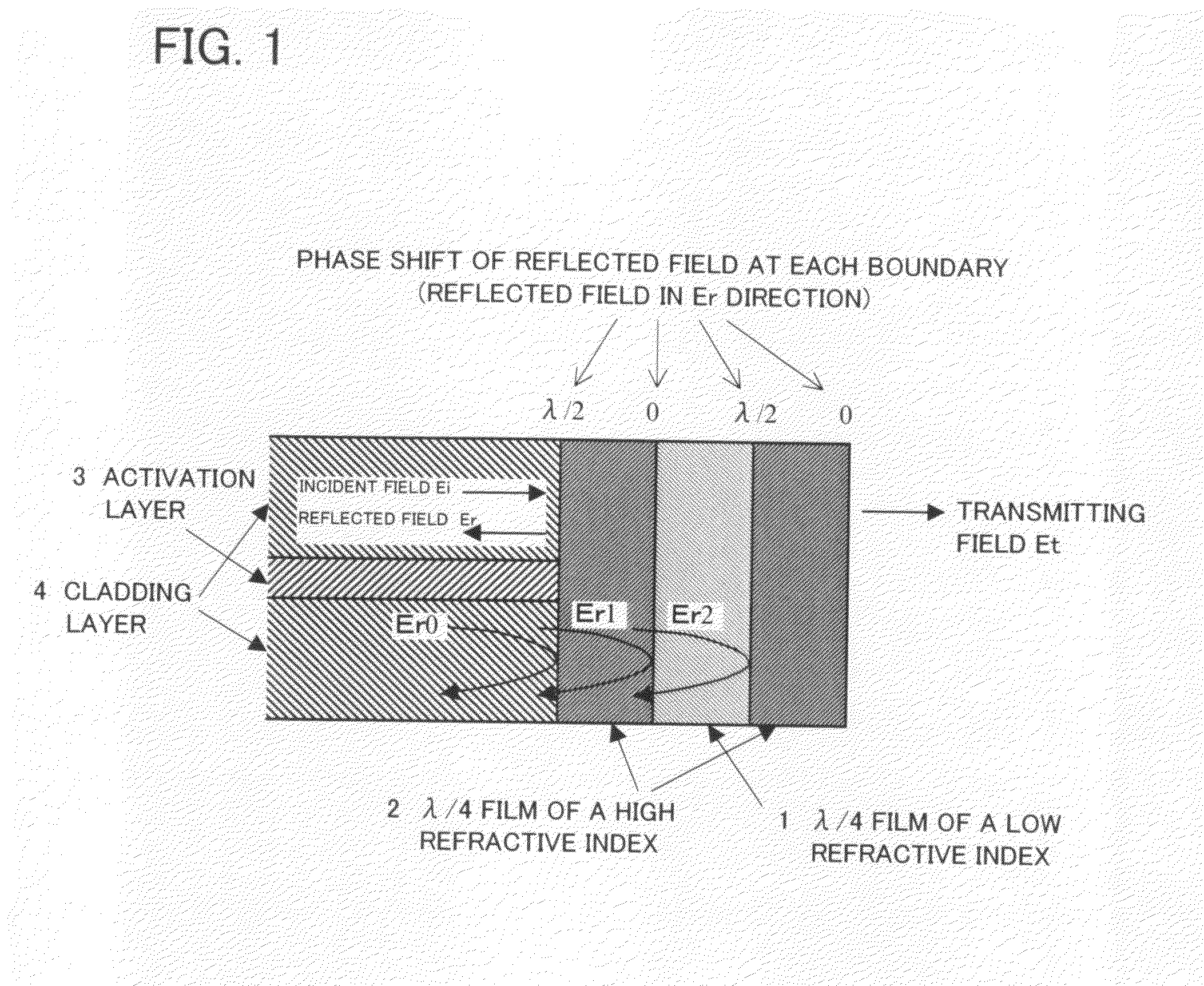
[0075]FIG. 3 illustrates a sectional view of a semiconductor laser element according to Example 1 of the present invention. The semiconductor laser resonator is made of a stack (laminate) including n-InP cladding layer 16, AlGaInAs multiple-quantum well activation layer 15, p-InP cladding layer 14 and p-InGaAs contact layer 13, stacked on an n-InP substrate 17, and further N-terminal 18 and P-terminal 12 so as to sandwich the stack. Coating films 5-11 are also formed at both facets of the resonator. High refractive index coating films 5, 7, 9 and 11 are made of amorphous Si (a-Si) and their thickness is 92.9 nm each whose optical path length is equal to λ / 4 of an oscillation wavelength λ=1.3 μm. Low refractive index coating films 6, 8 and 10 are made of Al2O3 and their thickness is 197 nm each whose optical path length is equal to λ / 4. Refractive indexes (N) of the amorphous Si (a-Si) and Al2O3 are 3.5 and 1.65, respectively. The front facet of the resonator is coated with four laye...

example 2

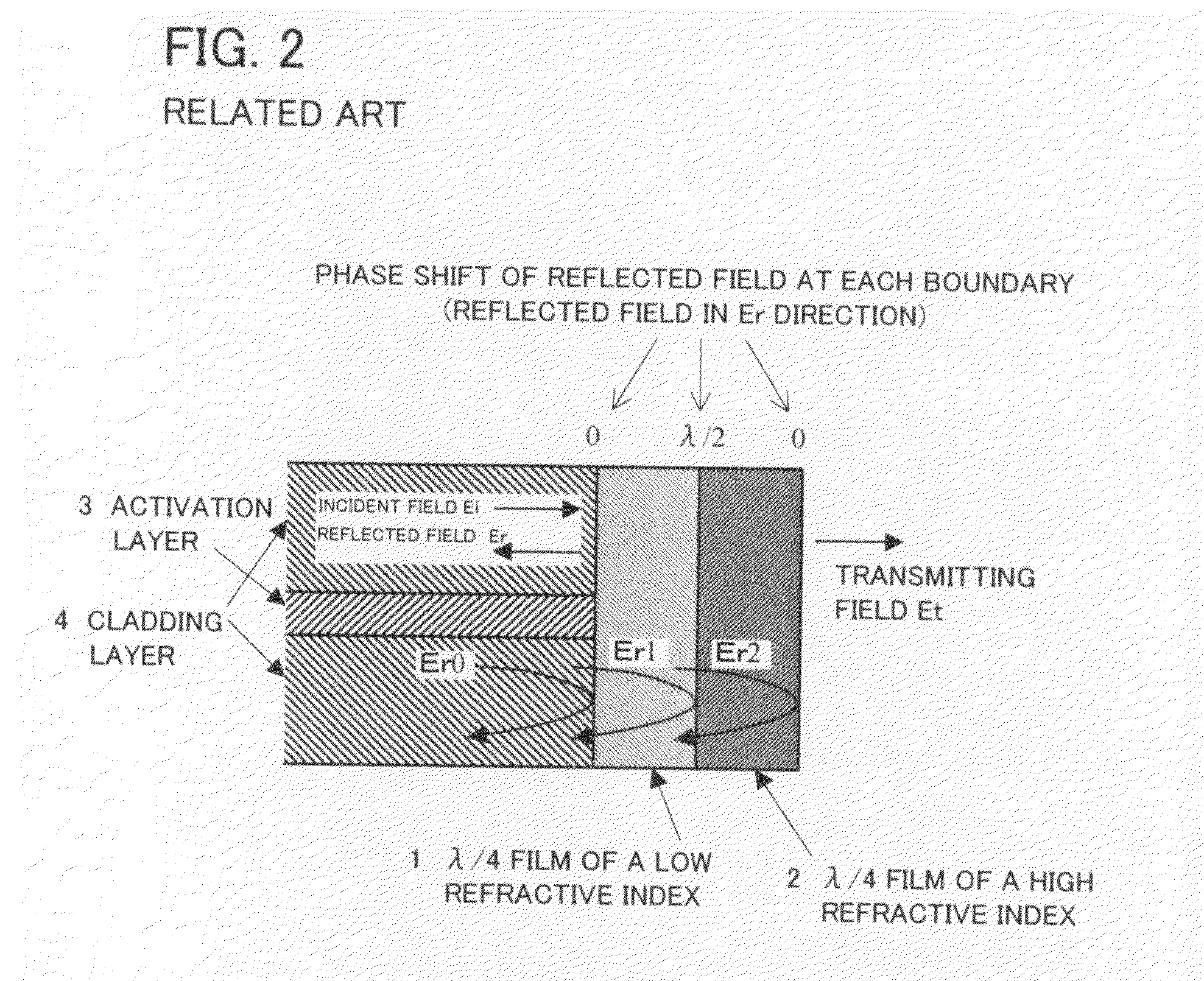
[0082]Although, the first layer adjacent to the semiconductor of Example 1 has a high refractive index as shown in FIG. 3, it is also possible to make the first layer as a low refractive index layer. FIG. 7 illustrates a cross sectional view of a semiconductor laser element according to Example 2 of the present invention, the first layer of which is a low refractive index layer. The semiconductor laser resonator is made of n-InP cladding layer 16, AlGaInAs multiple-quantum well activation layer 15, p-InP cladding layer 14, p-InGaAs contact layer 13, and P-terminal 12 are stacked on an n-InP substrate 17, in this order, provided that N-terminal 18 is formed on the other side of the substrate 17. And coating films 19 and 5-11 are formed at the both facets of the resonator. Both first coating films 19 adjacent to the semiconductor are made of Al2O3 and each thickness of the films is 394 nm, whose optical path length is λ / 2 relative to an oscillation wavelength λ=1.3 μm. The structures ...

example 3

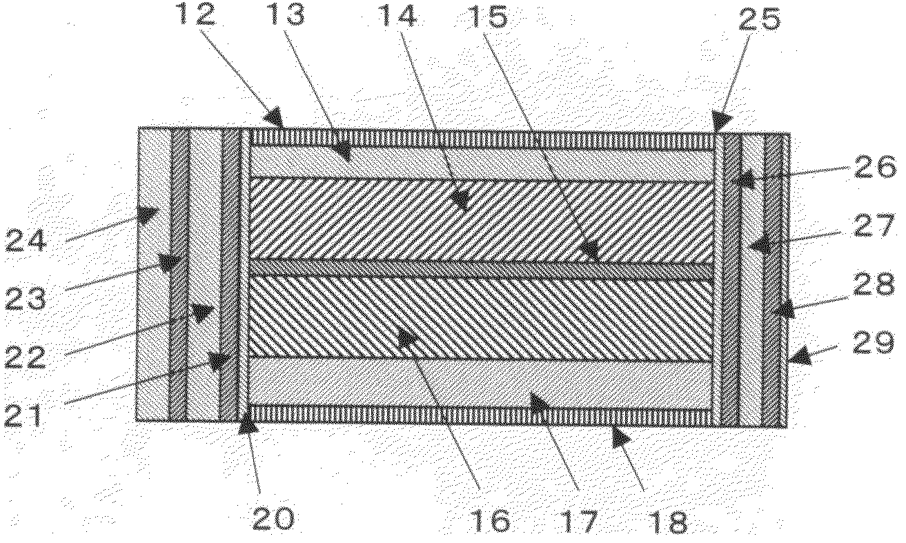
[0084]FIG. 8 illustrates a cross sectional view of a semiconductor laser element according to Example 3 of the present invention, the first layer of which is a low refractive index layer. The semiconductor laser resonator is made of n-InP cladding layer 16, AlGaInAs multiple-quantum well activation layer 15, p-InP cladding layer 14, p-InGaAs contact layer 13, and P-terminal 12 stacked, in this order, on an n-InP substrate 17, and N-terminal 18 stacked on the other side of the substrate 17. And coating films 20-29 are formed at the both facets of the resonator. The films 22, 24, 27 and 29 are low refractive index layers and made of Al2O3 whereas the films 21, 23, 26 and 28 are high refractive index layers and made of amorphous Si (hereafter referred to as ‘a-Si film’). The films 20 and 25 are thin films and made of Al2O3. The thicknesses of layers at the front facet (left side in FIG. 8) are; 20: Al2O3 film (30 nm), 21: a-Si film (74 mm), 22: Al2O3 film (157 nm), 23: a-Si film (74 nm...


PUM


Abstract

A semiconductor laser element realizes a high COD light output in broader range of reflection factor at a facet with high reliability. A semiconductor laser element has a multi-layered reflection film formed on at least one end facet of a resonator. An optical path length of each layer of said multi-layered reflection film is determined by (2m−1)·λ / 4, where λ is oscillation wavelength, and m is positive integer). A high-refractive-index layer and a low-refractive-index layer are alternately stacked starting from a first layer adjacent to said semiconductor.

Description

REFERENCE TO RELATED APPLICATION[0001]This application is based upon and claims the benefit of the priority of Japanese patent application No. 2007-063718, filed on Mar. 13, 2007, the disclosure of which is incorporated herein in its entirety by reference thereto.[0002]This invention relates to a highly reliable semiconductor laser element that has less facet damage and high resistance against electrostatic breakdown, and a method for producing same.FIELD OF THE INVENTIONBackground of the Invention[0003]A semiconductor laser is broadly utilized for optical communications, optical discs and light sources for measuring instruments due to its small size and high efficient performance. It is necessary for the semiconductor laser to control a reflection factor at an end facet (termed as “facet” hereinafter) of a resonator to obtain a low oscillation threshold and desired slope efficiency. A multiple layered film is generally used for the control of the reflection factor at a facet of a r...

Claims


Application Information

Patent Timeline
Patent Type & Authority Patents(United States)
IPC IPC(8): H01S3/08
CPCH01S5/028
Inventor ISHIKAWA, SHIN
Owner RENESAS ELECTRONICS CORP
Why Eureka
Try Eureka