Mesh structure and field-emission electron source apparatus using the same

a technology of electron source and mesh structure, which is applied in the manufacture of electric discharge tubes/lamps, instruments, discharge tubes luminescnet screens, etc., can solve the problems of increasing the size of imaging pixel, difficult to achieve the high-definition field-emission electron source display apparatus and the high-definition field-emission electron source imaging apparatus, and reducing the amount of electron beam reaching the target. , the effect of suppressing the decrease in the amount of electron beam

Inactive Publication Date: 2010-11-02
PANASONIC HEALTHCARE HLDG CO LTD +1
View PDF33 Cites 19 Cited by
  • Summary
  • Abstract
  • Description
  • Claims
  • Application Information

AI Technical Summary

Benefits of technology

[0060]In other words, it is an object of the present invention to provide a mesh structure that has a mechanical strength, emits less gas even in a vacuum and can be provided with through holes with an excellent dimensional accuracy.
[0061]Also, it is a further object of the present invention to provide a high-performance field-emission electron source apparatus that suppresses a decrease in the amount of an electron beam reaching a target while securing a mechanical strength of an electrode provided with a large number of through holes disposed between a field-emission electron source array and the target, and suppresses expansion of the electron beam on the target.

Problems solved by technology

This is very disadvantageous for the field-emission electron source display apparatuses and the field-emission electron source imaging apparatuses in which there is a demand for a uniform image.
However, in the conventional field-emission electron source apparatuses, since the distance between the field-emission electron source array and the target 103 may have variations of about several hundred micrometers to several millimeters, it is difficult to achieve the high-definition field-emission electron source display apparatus and the high-definition field-emission electron source imaging apparatus.
Consequently, there arises a problem that the size of an imaging pixel increases.
Further, in the case where an attempt is made to apply the field-emission electron source apparatus illustrated in FIG. 27 to a flat-type imaging apparatus for capturing an image of VGA (640 dots×480 dots, horizontally by vertically), the following problems may arise.
However, if the thickness of the shield grid electrode 120 is not greater than 1 μm, the shield grid electrode 120 is very likely to have problems of insufficient strength and warping.
However, the general assembling accuracy at present has a limit of about 1 μm.
In view of this, it also is considered difficult to achieve a flat-type imaging apparatus using the field-emission electron source apparatus illustrated in FIG. 27.
However, in view of the fact that current emission characteristics of the field-emission cold cathode element are on the order of nanoampares, it is considered difficult to achieve a field-emission electron source apparatus in which only a single cold cathode element 124 is arranged in a single pixel.
Accordingly, in this case, it also is considered difficult to achieve a field-emission electron source apparatus.
Furthermore, the field-emission electron source apparatus illustrated in FIG. 27 has another problem described below.
Moreover, the field-emission electron source apparatus illustrated in FIG. 27 has another problem described below.
Also, when a thinner glass sheet is prepared and provided with a large number of minute through holes 120a, there arises a problem that the mechanical strength of the glass deteriorates remarkably, so that the glass sheet becomes easy to crack.
Moreover, in the shield grid electrode 120 produced by forming a film of a metal or an alloy on a ceramic surface provided with a large number of through holes, there are problems that the ceramic needs a burning process, the distance between the adjacent through holes 120a is difficult to reduce, the mechanical strength is insufficient similarly to the case of using glass, etc.
However, the use of such a base material leads to the following problems.
However, it is difficult to use a current hole processing technique using a die or the like, and a small diameter of the through hole cannot be achieved by that technique.
Also, in the case of using glass as the material for the mesh structure, hole processing is difficult, and there are concern about gas emission in a vacuum and the problem of insufficient mechanical strength, similarly to the above.
Further, in the case of using ceramics as the material for the mesh structure, the following problem occurs.
That is, in order to secure the mechanical strength, it is difficult to reduce the intervals between the through holes.
Additionally, ceramics generally develop dimensional variations due to burning and thus make it difficult to control the through hole dimensions in a highly accurate manner.
Therefore, the ceramics are not suitable for filters whose through hole diameter has to be determined in a highly accurate manner with respect to the size of particles.

Method used


Image

  • Mesh structure and field-emission electron source apparatus using the same
  • Mesh structure and field-emission electron source apparatus using the same
  • Mesh structure and field-emission electron source apparatus using the same

Examples


embodiment 1

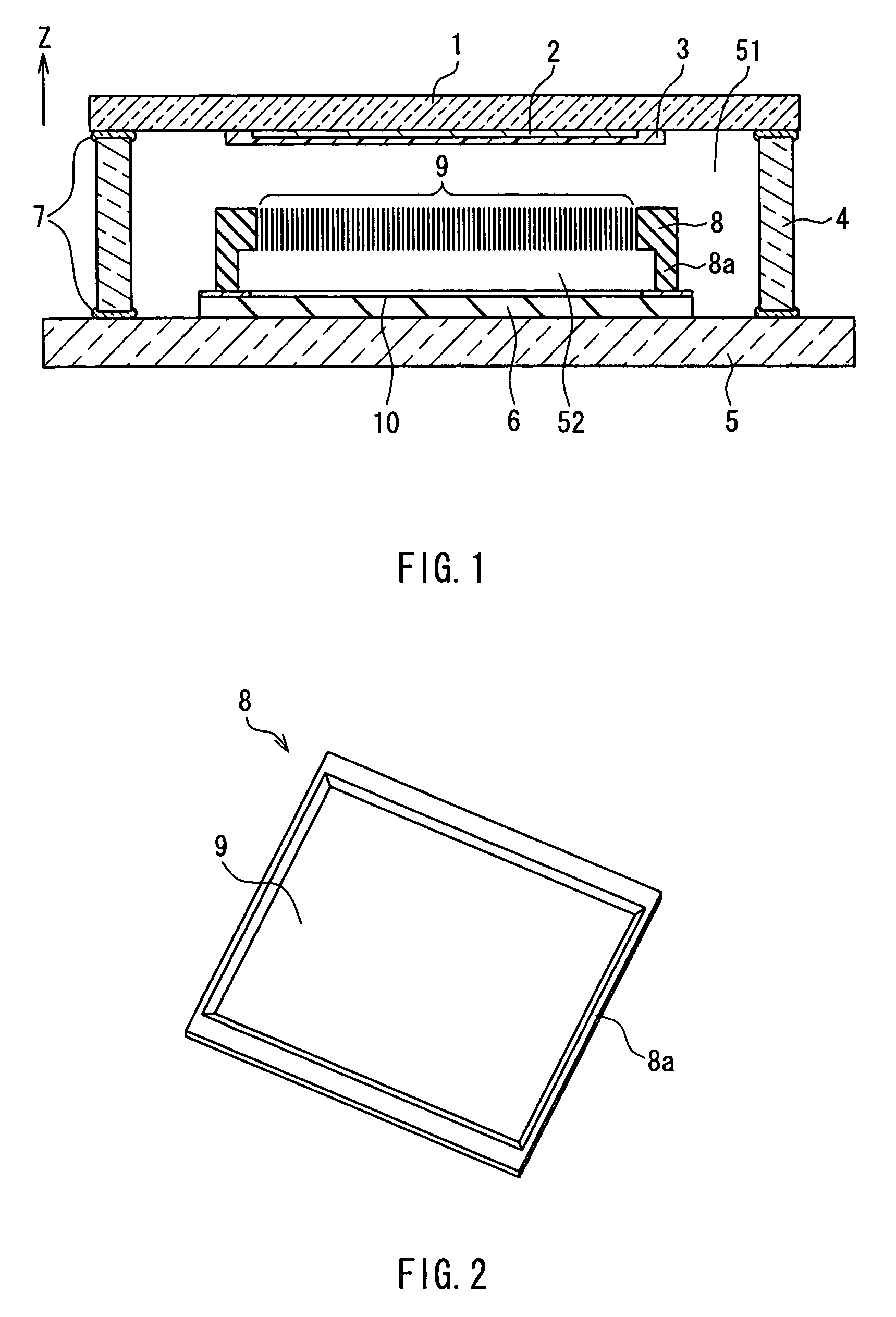
[0174]FIG. 1 is a sectional view showing a mesh structure and a field-emission electron source apparatus including the mesh structure according to Embodiment 1 of the present invention.

[0175]As shown in FIG. 1, a field-emission electron source apparatus according to Embodiment 1 of the present invention is provided with a vacuum container including a front panel 1 formed of light-transmitting glass, a back panel 5 and a wall part 4. Using a vacuum sealant 7, for example, frit glass for high-temperature burning or indium for low-temperature sealing, the front panel 1 and the wall part 4 are fixed firmly and sealed, and the back panel 5 and the wall part 4 are fixed firmly and sealed, so that the inside of the vacuum container is maintained under vacuum. For convenience of description in the following, an axis parallel with a direction normal to the front panel 1 and the back panel 5 is referred to as a Z axis.

[0176]An inner surface of the back panel 5 is provided with a semiconductor...

embodiment 2

[0278]FIG. 12 is a sectional view showing a mesh structure and a field-emission electron source apparatus including the mesh structure according to Embodiment 2 of the present invention.

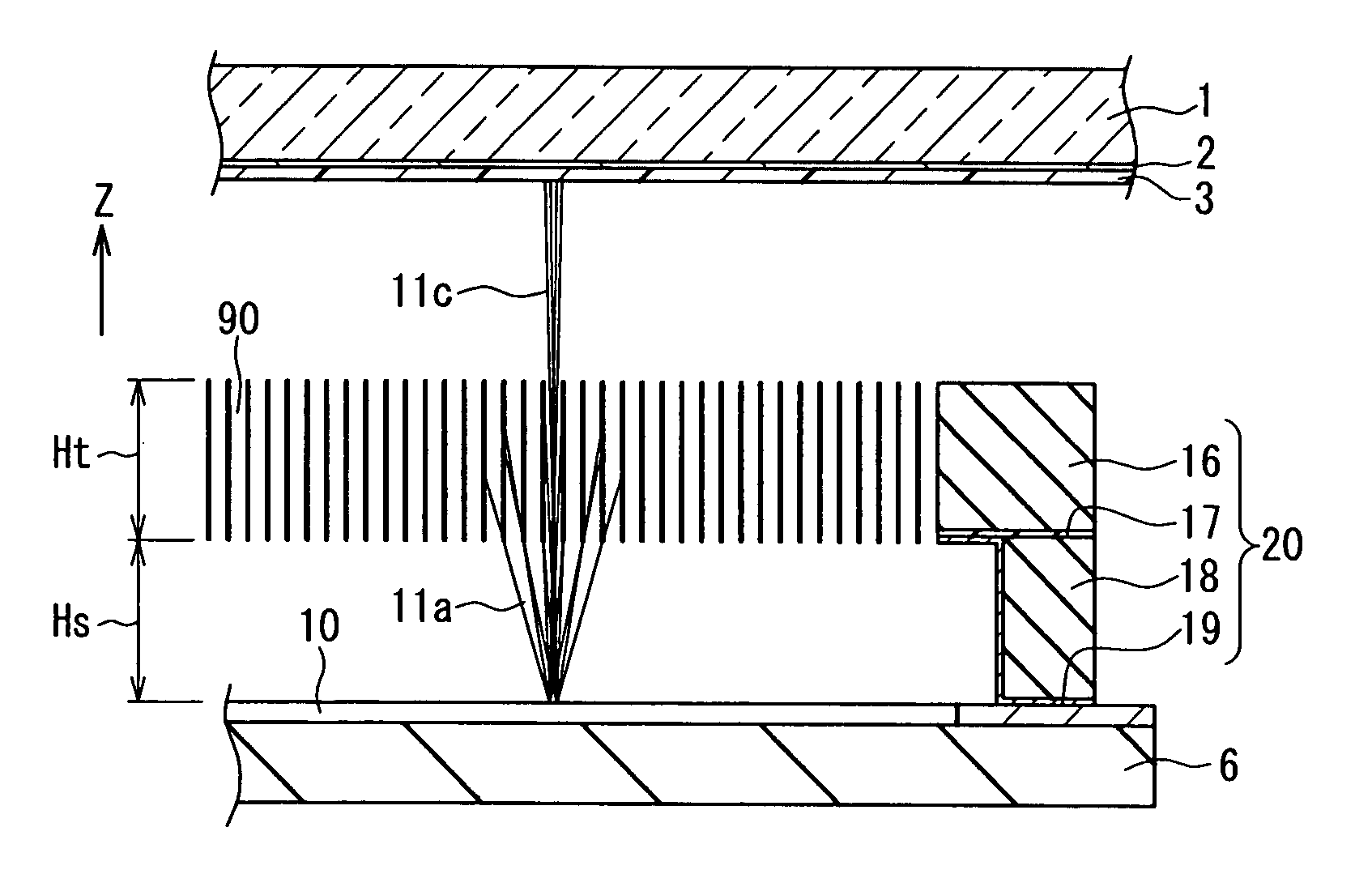
[0279]As shown in FIG. 12, the field-emission electron source apparatus according to Embodiment 2 of the present invention is different from that according to Embodiment 1 in that a mesh structure 20 has a three-layer structure unlike the mesh structure 8. In the following, the description of portions that are the same as those in Embodiment 1 will be omitted.

[0280]As shown in FIGS. 12, 13, 14A and 14B, the mesh structure 20 according to Embodiment 2 of the present invention has the three-layer structure including a first electrode layer 19 on a side of the field-emission electron source array, a second electrode layer 16 on a side of the target 3 and an insulating layer (intermediate layer) 17 therebetween. The insulating layer 17 ensures the insulation between the first electrode layer 19 and the s...

embodiment 3

[0320]FIG. 19 is a sectional view showing a mesh structure and a field-emission electron source apparatus including the mesh structure according to Embodiment 3 of the present invention.

[0321]As shown in FIG. 19, the field-emission electron source apparatus according to Embodiment 3 of the present invention is different from those according to Embodiments 1 and 2 in that a mesh structure 23 has a five-layer structure unlike the mesh structure 8 in Embodiment 1 and the mesh structure 20 in Embodiment 2. In the following, the description of portions that are the same as those in Embodiments 1 and 2 will be omitted.

[0322]As shown in FIGS. 19 and 20, the mesh structure 23 formed of the silicon-containing material according to Embodiment 3 of the present invention is obtained by providing a second insulating layer 21 and a third electrode layer 22 in this order on the surface of the mesh structure 20 on the side of the target 3 in Embodiment 2. The third electrode layer 22 is supplied wi...


PUM


Abstract

An electron beam emitted from a field-emission electron source array passes through a plurality of through holes formed in a mesh structure and reaches a target. Each of the plurality of through holes in the mesh structure has an opening on a side of the field-emission electron source array and an electron beam passageway that continues from the opening. The mesh structure is formed of a silicon-containing material doped with a N-type or P-type material. In this way, it is possible to suppress a decrease in the amount of the electron beam reaching the target while securing a mechanical strength of an electrode provided with a large number of through holes, and suppress expansion of the electron beam on the target.

Description

BACKGROUND OF THE INVENTION[0001]1. Field of the Invention[0002]The present invention relates to a mesh structure and a field-emission electron source apparatus using the same.[0003]2. Description of Related Art[0004]In recent years, with the development of fine processing technology for semiconductors, attention has been directed to a vacuum microelectronics technology of integrating a large number of minute cold cathode structures on the order of micrometers on a semiconductor substrate or the like. Field-emission electron source arrays including the minute cold cathode structures obtained by such a technology achieve flat-type electron emission characteristics and a high electric current density, and do not require a heat source such as a heater, unlike hot cathodes, thus offering potential as electron sources for a low-power-consumption next-generation flat display, sensors and electron sources for a flat-type imaging apparatus.[0005]As vacuum apparatuses using the field-emissio...

Claims


Application Information

Patent Timeline
Patent Type & Authority Patents(United States)
IPC IPC(8): H05H7/00
CPCH01J1/46H01J3/021H01J29/467H01J31/123
Inventor KIMIYA, JUNICHIKOGA, KEISUKEYAMAMOTO, MAKOTO
Owner PANASONIC HEALTHCARE HLDG CO LTD
Why Eureka
Try Eureka