
High density synapse chip using nanoparticles

a nanoparticle and high density technology, applied in the field of nanotechnology, can solve the problems of slow software simulation, unsuitable for many real-time problems of conventional computers, and proved extremely difficult, and achieve the effect of strengthening or weakening nanoconnections

Inactive Publication Date: 2010-11-02
KNOWM TECH
View PDF87 Cites 24 Cited by
  • Summary
  • Abstract
  • Description
  • Claims
  • Application Information

AI Technical Summary

Benefits of technology

"The present invention provides a physical neural network that can be formed and implemented using nanotechnology. The network can be formed from a plurality of interconnected nanoconnections or nanoconnectors, and can include neuron-like nodes and synapse chips. The network can be trained and used for various applications such as sensory processing, motor control, and pattern recognition. The invention also provides methods and systems for the training of multiple connection networks located between neuron layers within one or more multi-layer physical neural networks. The synapse chip includes an input layer and an output layer with a gap between them, and the network is formed by applying an electric field across the gap to create nanoconnections between the input and output electrodes. The strength of the nanoconnections can be controlled by adjusting the strength or frequency of the electric field. The invention provides a novel solution for creating a physical neural network with nanotechnology."

Problems solved by technology

In some applications, this has proved extremely difficult.
This makes conventional computers unsuitable for many real-time problems.
Software simulations are slow because during the learning phase a standard computer must serially calculate connection strengths.
When the networks get larger (and therefore more powerful and useful), the computational time becomes enormous.
For example, networks with 10,000 connections can easily overwhelm a computer.
Because software simulations are performed on conventional sequential computers, however, they do not take advantage of the inherent parallelism of neural network architectures.
Consequently, they are relatively slow.
Such speeds, however, currently require expensive super computers to achieve.
Even so, 18 million interconnects per second is still too slow to perform many classes of pattern classification tasks in real time.
The implementation of neural network systems has lagged somewhat behind their theoretical potential due to the difficulties in building neural network hardware.
Due to the difficulties in building such highly interconnected processors, the currently available neural network hardware systems have not approached this level of complexity.
Another disadvantage of hardware systems is that they typically are often custom designed and built to implement one particular neural network architecture and are not easily, if at all, reconfigurable to implement different architectures.
A true physical neural network chip, for example, has not yet been designed and successfully implemented.
The problem with pure hardware implementation of a neural network with technology as it exists today, is the inability to physically form a great number of connections and neurons.
On-chip learning can exist, but the size of the network would be limited by digital processing methods and associated electronic circuitry.
One of the difficulties in creating true physical neural networks lies in the highly complex manner in which a physical neural network must be designed and built.
However, it is becoming increasingly difficult to increase the number of elements on a chip using present technologies.
Present chip technology is also limited in cases where wires must be crossed on a chip.
For the most part, the design of a computer chip is limited to two dimensions.
This increases the cost and decreases the speed of the resulting chip.
Second, two wires can be selectively brought to a certain voltage and the resulting electrostatic force attracts them.
Such a device, however, is not well-suited for non-linear and analog functions.
To date, nanotechnology has not been applied to the creation of truly physical neural networks.

Method used


Image

  • High density synapse chip using nanoparticles
  • High density synapse chip using nanoparticles
  • High density synapse chip using nanoparticles

Examples


Embodiment Construction

[0054]The particular values and configurations discussed in these non-limiting examples can be varied and are cited merely to illustrate an embodiment of the present invention and are not intended to limit the scope of the invention.

[0055]The physical neural network described and disclosed herein is different from prior art forms of neural networks in that the disclosed physical neural network does not require computer calculations for training, nor is its architecture based on any current neural network hardware device. The design of the physical neural network of the present invention is actually quite “organic”. The physical neural network described herein is generally fast and adaptable, no matter how large such a physical neural network becomes. The physical neural network described herein can be referred to generically as a Knowm™. The terms “physical neural network” and “Knowm” can thus be utilized interchangeably to refer to the same device, network, or structure. The term “...


PUM


Abstract

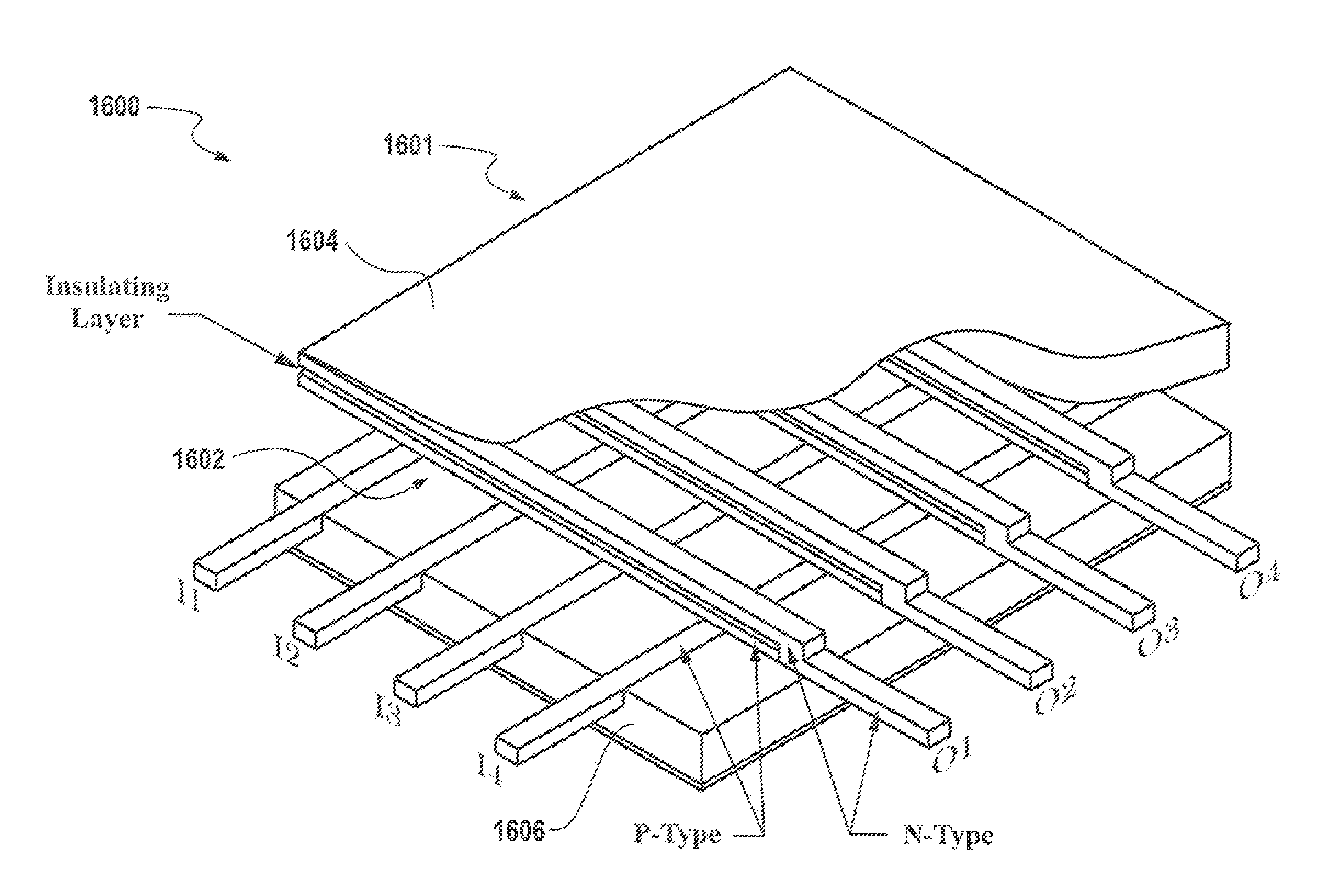
A physical neural network synapse chip and a method for forming such a synapse chip. The synapse chip can be configured to include an input layer comprising a plurality of input electrodes and an output layer comprising a plurality of output electrodes, such that the output electrodes are located perpendicular to the input electrodes. A gap is generally formed between the input layer and the output layer. A solution can then be provided which is prepared from a plurality of nanoconductors and a dielectric solvent. The solution is located within the gap, such that an electric field is applied across the gap from the input layer to the output layer to form nanoconnections of a physical neural network implemented by the synapse chip. Such a gap can thus be configured as an electrode gap. The input electrodes can be configured as an array of input electrodes, while the output electrodes can be configured as an array of output electrodes.

Description

CROSS-REFERENCE TO RELATED PATENT APPLICATIONS[0001]This application is a continuation of U.S. patent application Ser. No. 10 / 748,546 filed Dec. 30, 2003, which was issued on Jun. 24, 2008 (U.S. Pat. No. 7,392,230) and claims priority as a Continuation-In-Part of U.S. patent application Ser. No. 10 / 226,191 filed Aug. 22, 2002 which was abandoned on Jun. 28, 2007.TECHNICAL FIELD[0002]The present invention generally relates to nanotechnology. The present invention also relates to neural networks and neural computing systems and methods thereof. The present invention also relates to physical neural networks, which may be constructed based on nanotechnology. The present invention also related to VLSI (Very Large Scale Integrated) analog neural network chips. The present invention also relates to nanoconductors, such as nanotubes and nanowires. The present invention also relates to methods and systems for forming a neural network.BACKGROUND OF THE INVENTION[0003]Neural networks are compu...

Claims


Application Information

Patent Timeline
Patent Type & Authority Patents(United States)
IPC IPC(8): G06F15/18G06N3/06G06N3/063G06N99/00
CPCB82Y10/00G06N3/063G06N99/007G06N3/08G06N3/065
Inventor NUGENT, ALEX
Owner KNOWM TECH
Learn More