However, the biggest
disadvantage of CCD imagers is their small format and / or high price due to the fact that CCD sensors rely on specialized fabrication processes that require dedicated and costly manufacturing lines.
The drawbacks of CCD
imaging technology are the following:High-price due to specialized fabrication technology.High-
power consumption.Random pixel access is not possible, i.e., pixels must be read out sequentially, making it impossible for CCD imagers to easily access a subset of pixels within an image.Low yields that are caused by a huge area (over 50%) of the imager being covered by a thin or inter-poly
oxide that is prone to
oxide punch-throughData is transferred from the imager in the form of analog charge packets.
Due to losses, there is a maximum safe shifting distance, limiting the practical size of the
image sensor.Relatively slow frame rates.
For example,
CMOS image sensors can be made at standard manufacturing facilities that produce almost 90% of all
semiconductor chips, which significantly decreases their design and manufacturing costs.
In the APS design, the
photodetector is isolated from the readout lines reducing
crosstalk and
charge loss, which was a significant drawback of previous Passive Pixel Sensor designs.
Although APS designs have been able to realize many of the advantages associated with CMOS image sensors,
process variation in the transistors located at the pixels cause relatively high DC offset and
gain variation related
fixed pattern noise (FPN) as opposed to CCD's that intrinsically have low FPN due to the absence of
active devices at the pixels.
Furthermore, the minimum size readout transistors used in APS pixel designs introduce excess 1 / f
noise and thermal channel
noise thereby reducing the
dynamic range of CMOS imagers, which remains less than the
dynamic range of CCD imagers.
However, even though the 1 / f
noise is differentiated, it is poorly attenuated because the 1 / f noise samples are weakly correlated due to the relatively large time interval between samples.
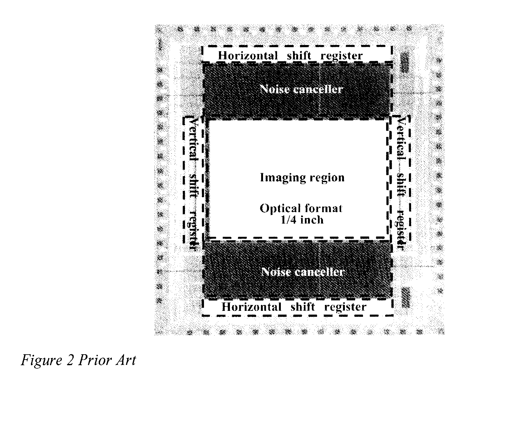
The capacitive elements could be placed external to the pixel area; however, this approach may be prohibitively expensive in terms of
silicon area and it has been shown that the CDS circuits may require as much area as the imaging region itself, see FIG. 2 for an example.
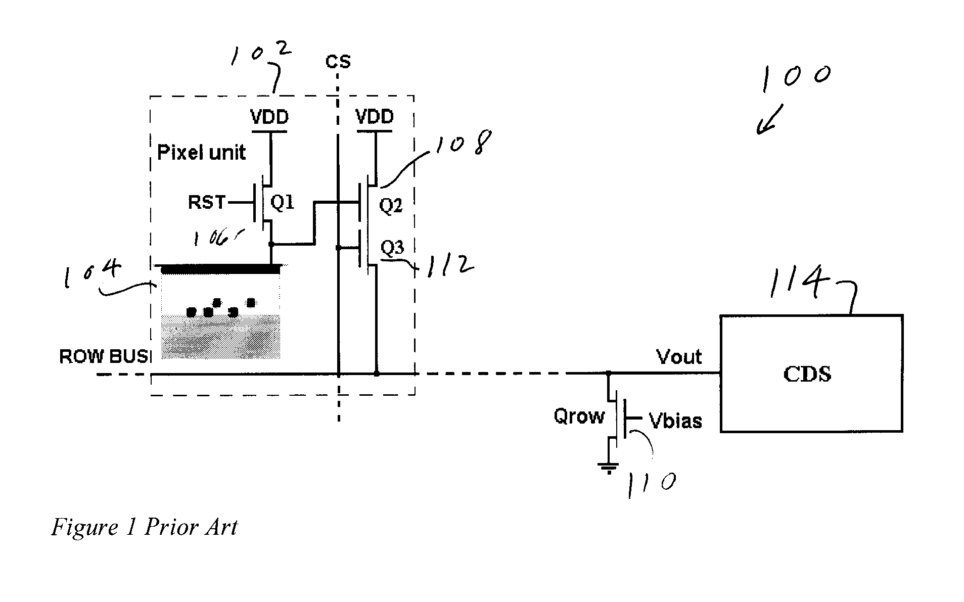
Another important
disadvantage of conventional APS image sensors, which are based on a source-follower
amplifier at each pixel site, is the relatively large
gain error among the pixels of the imager.
For example for the numbers given above, a 10% change in
transconductance results in a 2% change in the
closed loop gain, A. Another important disadvantage of the conventional APS structure is that its speed is limited by the current driving capabilities of the in-pixel source-follower
transistor, which usually is chosen to be a minimum size transistor to maintain high
fill factor.
Therefore, the small in-pixel transistor of the standard APS limits the speed of the imager—more specifically it slows down positive
voltage transients on the readout lines.
Hence, the limited speed problem becomes more prominent as the CMOS technology is scaled and the pixel count of the image sensor increases, specifically more pixels must be read while maintaining the same number of frames per second, therefore each pixel must be read faster.
Limited readout speed reduces the performance of
correlated double sampling because the two consecutive samples cannot be obtained quickly enough (the sampling speed becomes slower than 1 / f noise corner frequency) resulting in leakage of the 1 / f
noise power into the
signal band.
While the
negative voltage swings on the readout-lines could be sped up by increasing the biasing current value in the standard APS designs, the positive swings are always limited by the size of the small in-pixel transistor.
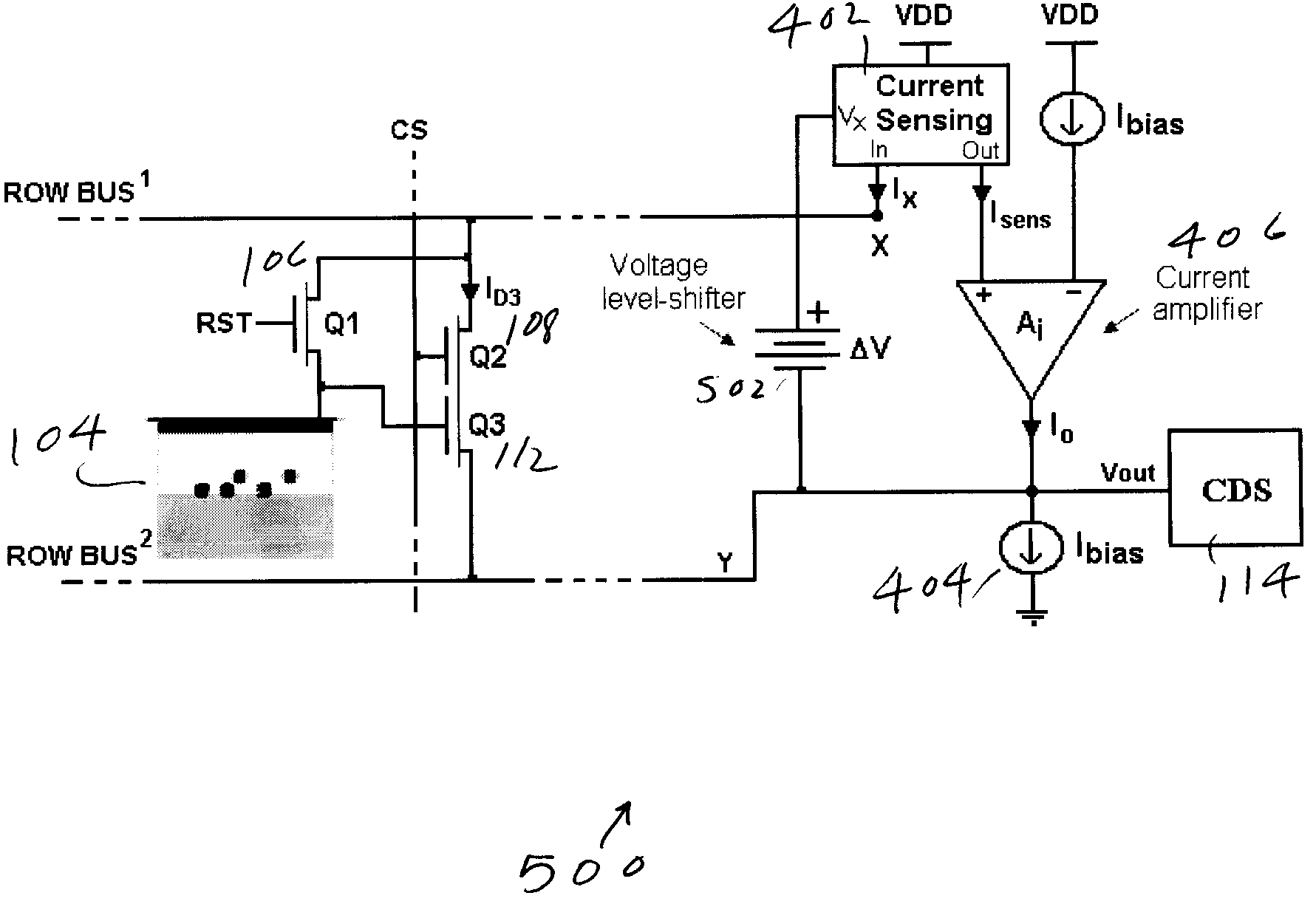
However, the overall speed improvement of the ACS is rather modest because the
parasitic capacitance of the ROW-
BUS2 line is still driven by the small size transistor Q5 that has to be matched to the in-pixel transistor Q3.
This
bus line, which heavily loads the transistor Q5 and has to follow output value changes, slows down the overall response.
Therefore, as the CMOS technology continues to scale, the ACS is facing the same speed limitation problem as the standard APS.

