One-transistor cell semiconductor on insulator random access memory

a semiconductor and random access memory technology, applied in the field of dielectric charge trapping memory technology, can solve the problems of limiting the total programming throughput of nor flash, affecting the performance of the memory, and consuming relatively large amounts of power,

Active Publication Date: 2010-12-07
MACRONIX INT CO LTD
View PDF82 Cites 6 Cited by
  • Summary
  • Abstract
  • Description
  • Claims
  • Application Information

AI Technical Summary

Benefits of technology

[0015]In alternative embodiments, an ultra-thin tunnel oxide is implemented providing for very fast program / erase operations, supported by refresh operations as used in classical DRAM technology.
[0016]In other alternative embodiments, no tunnel oxide is implemented providing for very fast program / erase operations so that the charge trapping layer is in contact with the gate for gate injection operation, or the channel for channel injection, and the charge trapping is supported by refresh operations as used in classical DRAM technology. The gate injection embodiment allows operation in modes avoiding tunneling damage to the oxide contacting the channel. The memory cells in the arrays described herein comprise a single transistor, so the scaling capability should be superior to the current DRAM technology, where a larger-area capacitor is required. For the DRAM embodiments, a “SONS” structure is described using use gate-injection to program and erase the memory cell. Without any “tunnel oxide” (relative to the gate) high program / erase speeds are achieved. By avoiding passing current through the gate oxide, very high endurance (>10G times) is achieved. Even without the top oxide, the silicon nitride trapping provides sufficient data retention for DRAM. Silicon rich nitride is utilized in embodiments described herein for improved performance. Also, p-channel implementations are described.

Problems solved by technology

CHE programming consumes relatively large amounts of power, limiting the total programming throughput for NOR Flash.
Moreover, hot-carrier injection often has relatively poor program and erase P / E endurance, since the high-energy carriers easily damage the tunnel oxide.
Therefore, NAND Flash has the drawback that random access read is impractical.
However, NOR and NAND Flash do not support random bit-by-bit erase operations.
Therefore, Flash memory has not been applied for applications requiring random read and write operation at high speeds.
However, slow erase speeds still limit application of AND architecture devices to applications that do not require high speed, random write access.
The scaling of the conventional one-transistor, one capacitor 1T1C DRAM memory has become very difficult since the cell capacitance is not scalable.
However, it is very difficult for an FBC to achieve good data retention because junction leakage easily bleeds the storage node.
However, during program / erase operation current flows through the gate oxide (tunnel oxide) and causes damage to the gate oxide.
Therefore, SONOS devices have relatively poor endurance of 7 cycles.

Method used


Image

  • One-transistor cell semiconductor on insulator random access memory
  • One-transistor cell semiconductor on insulator random access memory
  • One-transistor cell semiconductor on insulator random access memory

Examples


Embodiment Construction

[0048]A detailed description of embodiments of the present invention is provided with reference to the FIGS. 1-23.

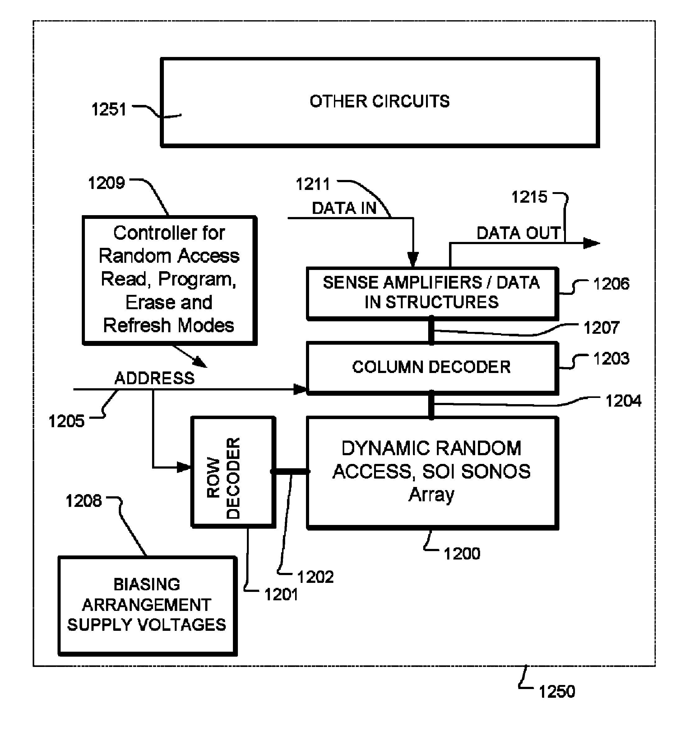
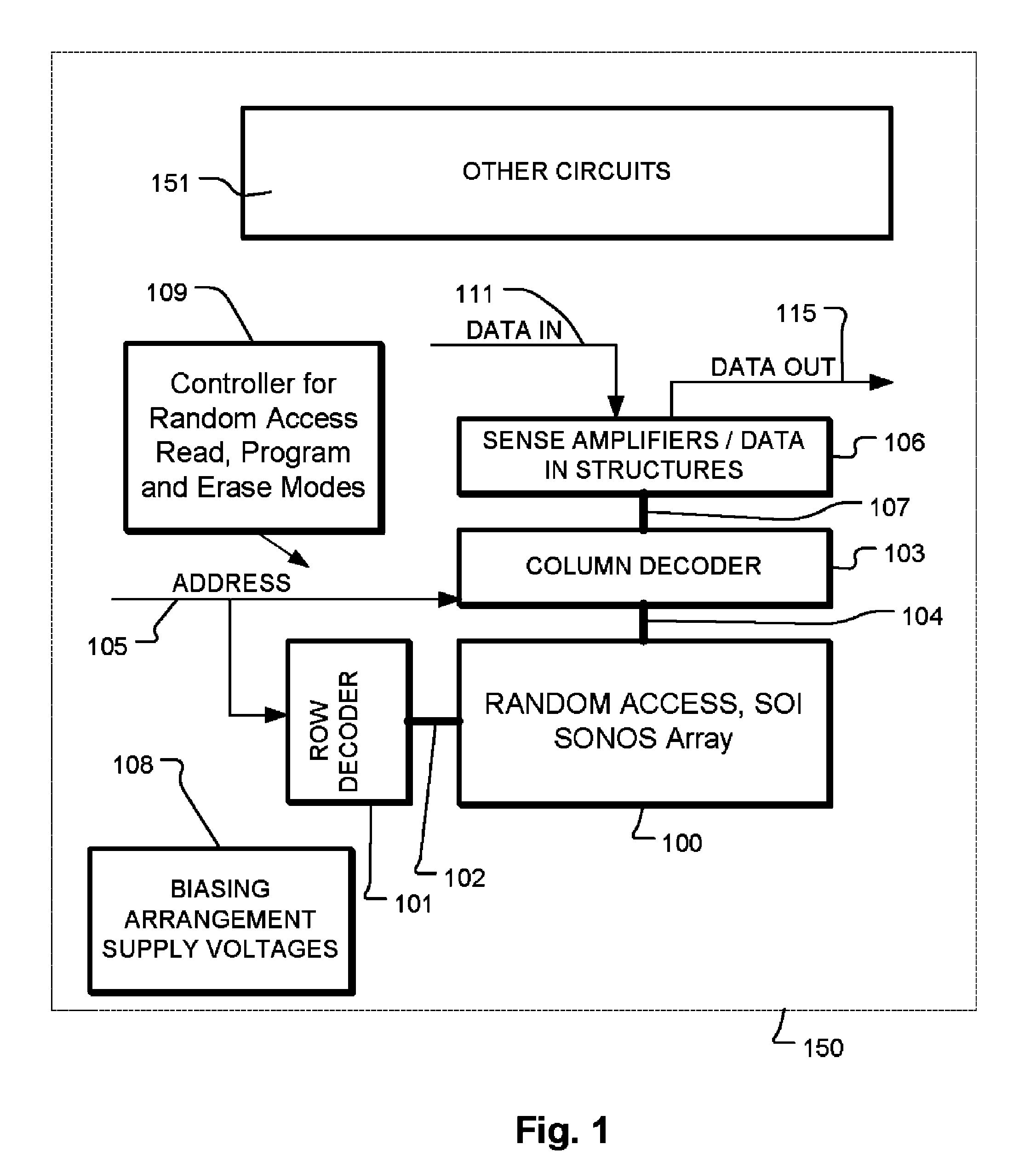
[0049]FIG. 1 is a simplified block diagram of an integrated circuit 150 including a substrate which may be a single chip or multiple chips adapted for packaging together in a single integrated circuit package, and a memory array 100 in a first region of substrate which comprises an array of one-transistor, dielectric charge trapping memory cells arranged in a divided bit line architecture in a SOI configuration, and adapted for random access read, erase and program operations. A word line (or row) and block select decoder 101 is coupled to, and in electrical communication with, a plurality 102 of word lines and block select lines, and arranged along rows in the memory array 100. A bit line (column) decoder and drivers 103 are coupled to and in electrical communication with a plurality of bit lines 104 arranged along columns in the memory array 100 for reading data from, ...


PUM


Abstract

Silicon-oxide-nitride-oxide-silicon SONOS-type devices (or BE-SONOS) fabricated in Silicon-On-Insulator (SOI) technology for nonvolatile implementations. An ultra-thin tunnel oxide can be implemented providing for very fast program / erase operations, supported by refresh operations as used in classical DRAM technology. The memory arrays are arranged in divided bit line architectures. A gate injection, DRAM cell is described with no tunnel oxide.

Description

[0001]The benefit is claimed in present application of U.S. Provisional Application No. 61 / 019,383, filed 7 Jan. 2008; and of U.S. Provisional Application No. 60 / 980,795, filed 18 Oct. 2007; both of which are incorporated by reference as if fully set forth herein.BACKGROUND OF THE INVENTION[0002]1. Field of the Invention[0003]The present invention relates to dielectric charge trapping memory technology arranged for nonvolatile and dynamic random access applications.[0004]2. Description of Related Art[0005]Current flash memory products are typically implemented using a NOR architecture or a NAND architecture.[0006]For NOR architecture flash, the memory transistors are connected in parallel, so that large reading current can be provided (typically larger than 20 μA). The large reading current provides fast random access read applications (typically 70-100 nsec for single bit reading). However, for NOR Flash, programming usually employs channel hot electron (CHE) injection. CHE program...

Claims


Application Information

Patent Timeline
Patent Type & Authority Patents(United States)
IPC IPC(8): G11C11/40G11C11/402
CPCG11C16/0466H01L21/84H01L27/108H01L27/10873H01L27/115H01L27/11568H01L27/1203H01L29/792H10B12/00H10B12/05H10B43/30H10B69/00
Inventor LUE, HANG-TING
Owner MACRONIX INT CO LTD
Why Eureka
Try Eureka