Method of increasing yield in OFETs by using a high-K dielectric layer in a dual dielectric layer

a dielectric layer and dielectric layer technology, applied in the field of organic fets, can solve the problems of increasing the probability of pinholes, increasing the probability of shorting between the first conductor source/drain layer, and reducing the performance of the transistor

Inactive Publication Date: 2010-12-21
GULA CONSULTING LLC
View PDF6 Cites 3 Cited by
  • Summary
  • Abstract
  • Description
  • Claims
  • Application Information

AI Technical Summary

Benefits of technology

[0009]According to the present invention, an OFET fabrication method provides a solution to the pinhole problem discussed above by depositing a second layer on top of the original dielectric layer, wherein the second dielectric layer has a significantly higher dielectric constant than that of the original dielectric constant layer. A dielectric layer with a high dielectric constant is referred to as a “high-K dielectric layer”. Electrically, the dual dielectric structure of the present invention can be thought of as a high-K dielectric capacitor in series with a low-K dielectric capacitor. In such a circuit configuration, the contribution of the high-K dielectric capacitor to the overall capacitance of the dual structure is minimal. Therefore, though the overall thickness of the dual dielectric structure is increased, the capacitance remains substantially unchanged. Consequently, pinhole density and the probability of shorts is decreased while not adversely affecting the performance of the dual-gate dielectric device.
[0012]The dielectric layer pinholes in prior art OFET structures are addressed through the addition of a high-K dielectric layer to eliminate the effects of shorts in the dielectric layer. In the claimed structure, the original dielectric layer is maintained such that the semiconductor / dielectric interface remains unchanged. The high-K dielectric layer contributes material to the gate dielectric to plug up pinholes in the original dielectric, but does not contribute significant capacitance due to the high dielectric constant of the additional dielectric layer. Thereby, the incidence of pinholes in the dielectric layer is reduced without significantly affecting the performance of the OFET transistor.

Problems solved by technology

However, as the dielectric layer is made thinner, there is an increased probability of shorting between the first conductor source / drain layer and the second conductor gate layer caused by an increased likelihood of pinholes in the thinner dielectric.
Such pinholes are particularly prevalent in polymer dielectric layers and will inadvertently permit shorting of a first layer conductor to a second layer conductor in the OFET.
However, both of these approaches undesirably result in a thicker gate dielectric layer, significantly decreasing the performance of the transistor.

Method used


Image

  • Method of increasing yield in OFETs by using a high-K dielectric layer in a dual dielectric layer
  • Method of increasing yield in OFETs by using a high-K dielectric layer in a dual dielectric layer
  • Method of increasing yield in OFETs by using a high-K dielectric layer in a dual dielectric layer

Examples


first embodiment

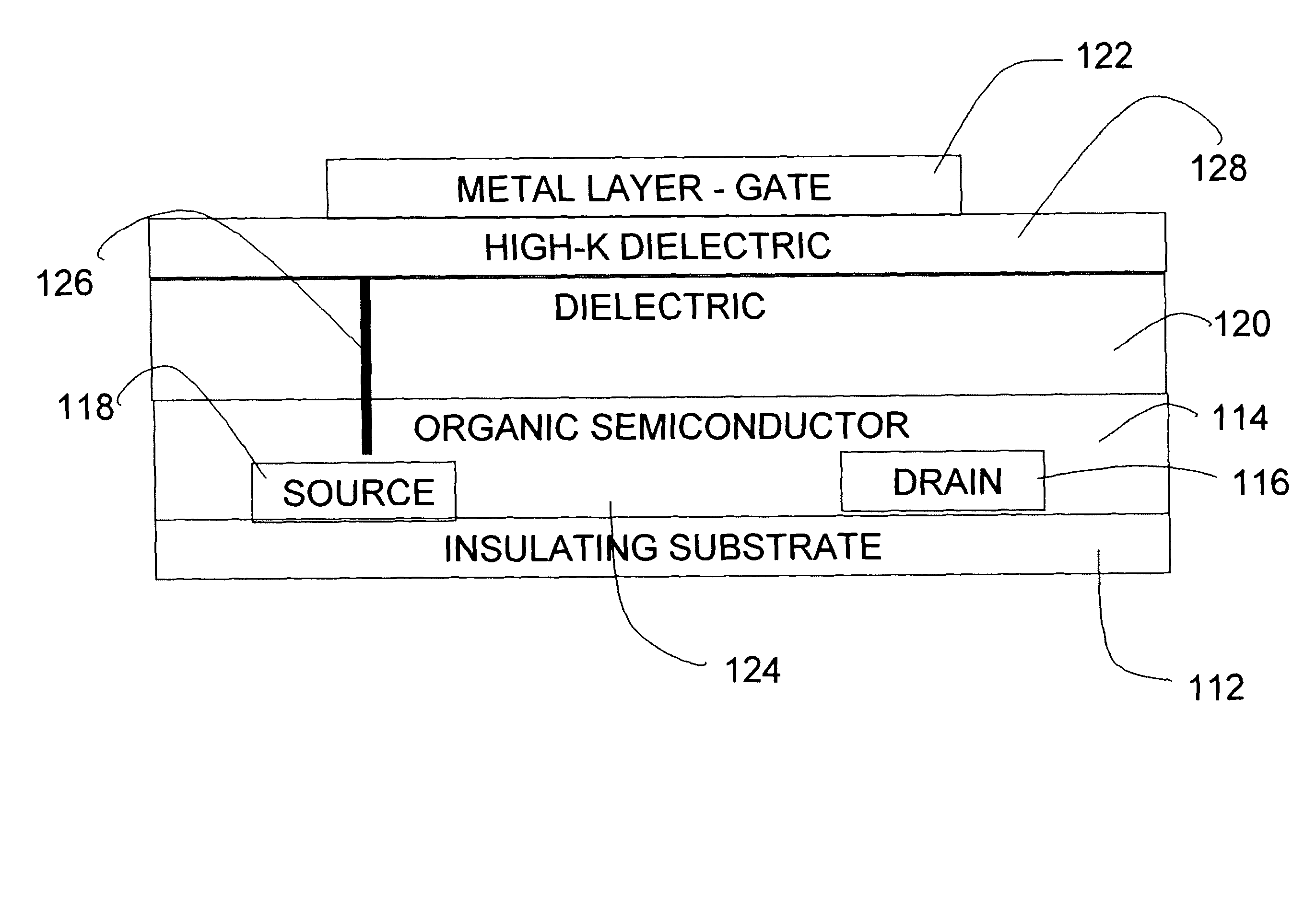
[0013]In the invention, a top gate OFET having a dual dielectric layer includes a patterned first conductive layer on an insulating substrate forming source and drain contacts, a semiconductor layer in a channel region between the source and drain contacts, a first dielectric layer over the semiconductor layer in at least the channel region as well as any unconnected first level metal areas, a second dielectric layer over the first dielectric layer in at least the channel region as well as any unconnected first level metal areas, and a patterned second conductive layer on the second dielectric layer over the channel region, wherein the second dielectric layer has a dielectric constant higher than that of the first dielectric layer.

second embodiment

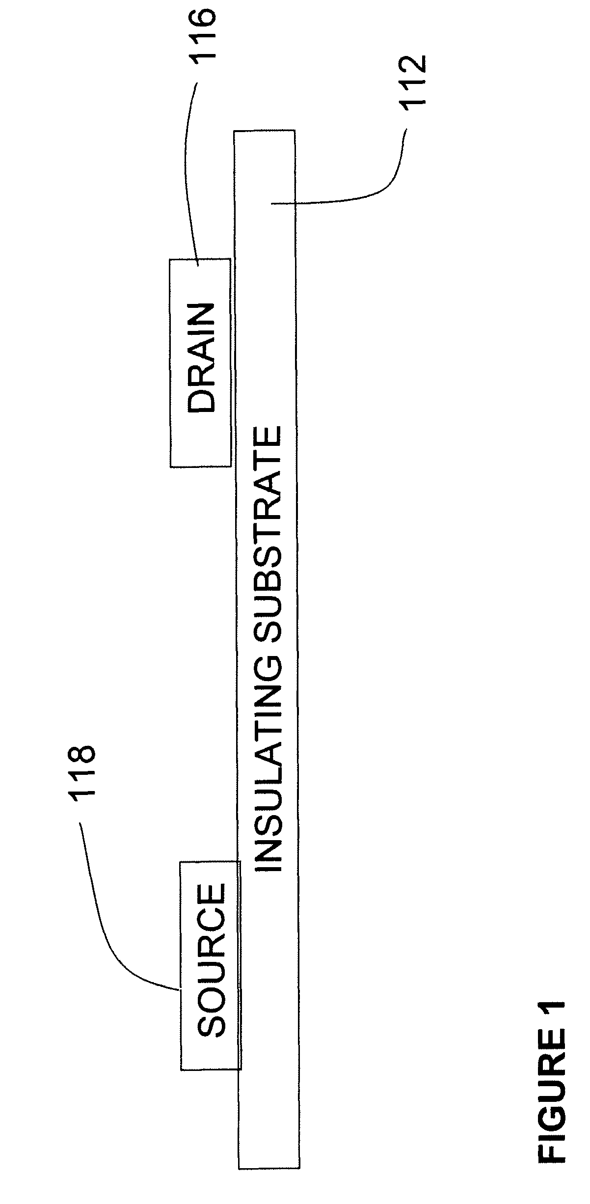
[0014]In the invention, a bottom-gate / bottom-contact OFET structure having a dual dielectric layer includes a patterned first conductive layer on an insulating substrate, a first dielectric layer over the patterned first conductive layer, a second dielectric layer over the first dielectric layer, a patterned second conductive layer on the second dielectric layer forming source and drain contacts, and an organic semiconductor layer in a channel region between the source and drain contacts, wherein the second dielectric layer has a dielectric constant higher than that of the first dielectric layer.

third embodiment

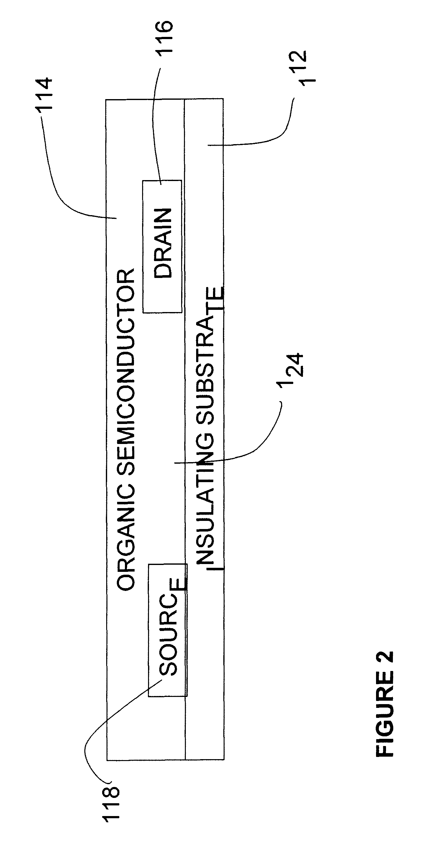
[0015]In the invention, a bottom-gate / bottom-contact OFET structure having a dual dielectric layer includes a patterned first conductive layer on an insulating substrate, a first dielectric layer over the patterned first conductive layer, a second dielectric layer over the first dielectric layer, an organic semiconductor layer over the second dielectric layer, and a patterned second conductive layer on organic semiconductor layer forming source and drain contacts, wherein the second dielectric layer has a dielectric constant higher than that of the first dielectric layer.

[0016]In the embodiments of the present invention, the insulating substrate includes PET, PEN, glass, or Kapton. The first conductive layer includes conductive organic materials such as PEDOT and carbon black, or nano-particle solutions or pre-cursors of inorganic materials such as gold, silver, titanium, aluminum, or silicon. The semiconductor layer includes an organic semiconductor such as polythiophene or solutio...


PUM

PropertyMeasurementUnit
dielectric constantaaaaaaaaaa
conductiveaaaaaaaaaa
insulatingaaaaaaaaaa

Abstract

Dielectric layer pinholes in OFET structures are addressed in a method of fabricating OFET devices through the addition of a high-K dielectric layer to eliminate the effects of shorts in the dielectric layer. The original dielectric layer is maintained such that the semiconductor / dielectric interface remains unchanged. The high-K dielectric layer contributes material to the gate dielectric to plug up pinholes in the original dielectric, but does not contribute significant capacitance due to the high dielectric constant of the additional dielectric layer. The incidence of pinholes in the dielectric layer is reduced without significantly affecting the performance of the OFET transistor.

Description

FIELD OF THE INVENTION[0001]The present invention relates to Organic FETs (“OFETs”), and, more particularly, to the use of a second, high-K dielectric layer in addition to a first, low-K dielectric layer in an OFET structure to improve reliability and yield without adversely affecting performance.BACKGROUND OF THE INVENTION[0002]The performance of an OFET structure is generally improved when the capacitance between the gate and the channel increases. This can be achieved by making the dielectric layer between the gate and channel as thin as possible. However, as the dielectric layer is made thinner, there is an increased probability of shorting between the first conductor source / drain layer and the second conductor gate layer caused by an increased likelihood of pinholes in the thinner dielectric.[0003]Such pinholes are particularly prevalent in polymer dielectric layers and will inadvertently permit shorting of a first layer conductor to a second layer conductor in the OFET. In the...

Claims


Application Information

Patent Timeline
Patent Type & Authority Patents(United States)
IPC IPC(8): H01L51/40
CPCH01L51/0533H10K10/476
Inventor DIMMLER, KLAUS
Owner GULA CONSULTING LLC
Why Eureka
Try Eureka