Method of manufacturing photoelectric conversion device

a technology of photoelectric conversion device and manufacturing method, which is applied in the manufacture of final products, basic electric elements, climate sustainability, etc., can solve the problem of difficult for a conventional apparatus to give a large amount of current, cycle time might decrease, and the depth of ion implantation in a single crystal silicon substrate is the upper limit of the depth of ion implantation, etc. problem, to achieve the effect of improving photoelectric conversion efficiency, suppressing resource consumption, and photoelectric conversion layer

Inactive Publication Date: 2010-12-28
SEMICON ENERGY LAB CO LTD
View PDF36 Cites 28 Cited by
  • Summary
  • Abstract
  • Description
  • Claims
  • Application Information

AI Technical Summary

Benefits of technology

[0011]When a hydrogen ion implantation separation method is employed, a single crystal silicon thin film which is homogeneous can be formed through a low-temperature process as compared with when a SIMOX substrate or a bonding substrate utilizing grinding or polishing is used. Furthermore, a single crystal silicon substrate from which a single crystal silicon thin film has been separated can be reused, which can achieve effective utilization of resources.
[0014]Utilizing a crystal solid phase growth technique, a single crystal semiconductor layer that forms a photoelectric conversion layer is made thick. Utilizing a bonding technique of different kinds of substrates, a single crystal semiconductor layer is formed over a supporting substrate. The single crystal semiconductor layer is obtained by slicing a single crystal semiconductor substrate. An amorphous semiconductor layer is formed on the single crystal semiconductor layer fixed to the supporting substrate and heat treatment is performed. The single crystal semiconductor layer that is in contact with the amorphous semiconductor layer serves as a seed crystal, and the amorphous semiconductor layer is subjected to solid phase growth, whereby single crystallization is performed. That is, the amorphous semiconductor layer becomes a single crystal semiconductor layer, and as a result, the single crystal semiconductor layer is made thick. By solid phase growth of the amorphous semiconductor layer, the single crystal semiconductor layer can be easily made thick.
[0023]Since the thickness of the single crystal semiconductor layer for forming the photoelectric conversion layer is increased in accordance with a crystal solid phase growth technique, it is possible to improve photoelectric conversion efficiency while suppressing the consumption of resources. Moreover, the consumption of a single crystal semiconductor, which is the material, can be reduced by slicing a superficial portion of a single crystal semiconductor substrate and bonding the portion to the supporting substrate as a single crystal semiconductor layer. Furthermore, the single crystal semiconductor substrate from which the single crystal semiconductor layer has been separated can be reused. Thus, the resources can be effectively utilized and a photoelectric conversion device having an excellent photoelectric conversion characteristic can be obtained.

Problems solved by technology

However, the acceleration voltage of an ion implantation apparatus has limitation in terms of the apparatus, so that there is the upper limit of the depth of ion implantation in a single crystal silicon substrate.
However, it was difficult for a conventional apparatus to give a large amount of current by increasing the acceleration voltage.
Therefore, when the acceleration voltage is increased, a long period of time is necessary in order to obtain a given implantation amount, which results in that the cycle time might decrease.

Method used


Image

  • Method of manufacturing photoelectric conversion device
  • Method of manufacturing photoelectric conversion device
  • Method of manufacturing photoelectric conversion device

Examples


embodiment mode 1

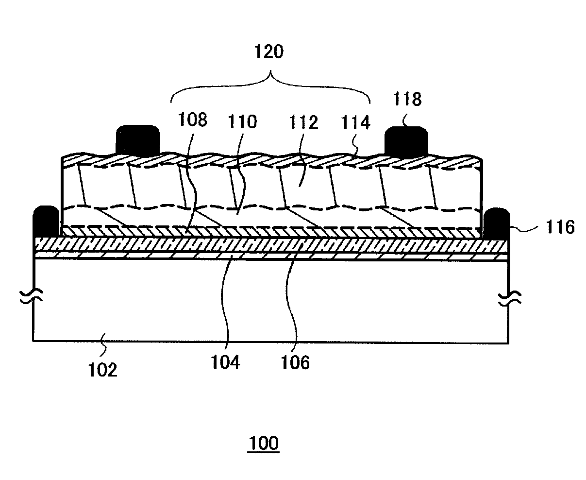
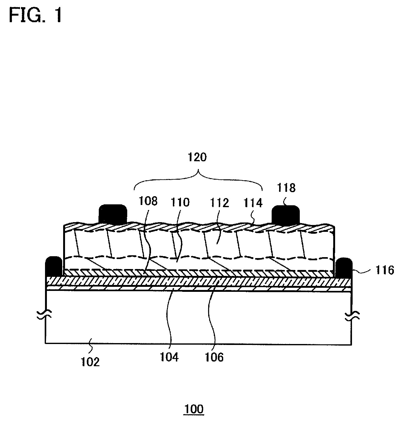
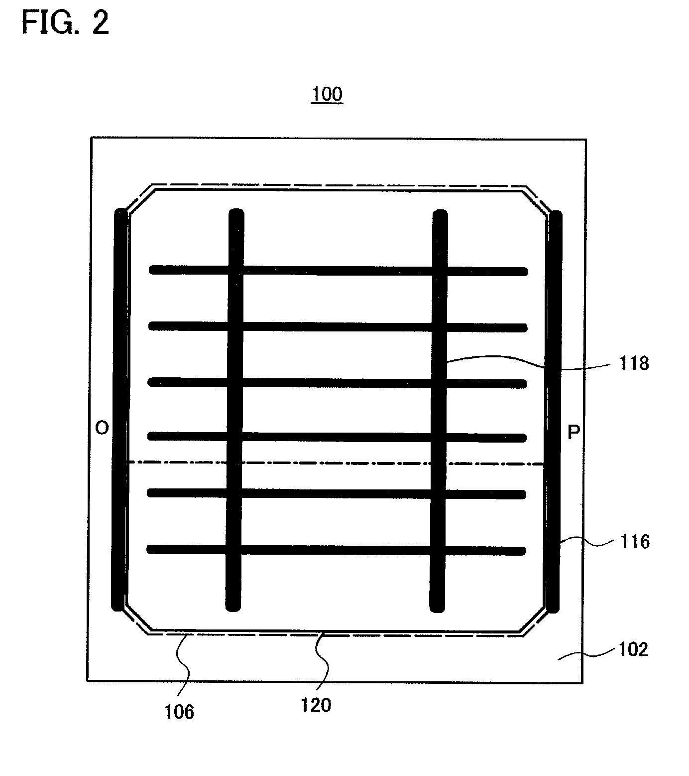
[0050]FIG. 1 is a schematic cross-sectional view of a photoelectric conversion device 100 according to this embodiment mode. FIG. 2 is a schematic top view of the photoelectric conversion device 100 according to this embodiment mode. Note that FIG. 1 illustrates an example of a cross-sectional view along a line O-P in FIG. 2.

[0051]The photoelectric conversion device 100 described in this embodiment mode includes a unit cell 120 fixed to a supporting substrate 102. The unit cell 120 includes a single crystal semiconductor layer. The unit cell 120 is provided with a first electrode 106 on the supporting substrate 102 side and with a second electrode 118 on the surface side of the unit cell 120. Moreover, an auxiliary electrode 116 is provided in electrical connection with the first electrode 106. The photoelectric conversion device 100 of this embodiment mode has a structure in which the unit cell 120 is fixed to the supporting substrate 102, and a positive electrode and a negative el...

embodiment mode 2

[0140]In this embodiment mode, an example of a method of manufacturing a photoelectric conversion device, which is different from that in Embodiment Mode 1, will be described. Specifically, the example of (1) about the formation order of the fragile layer 105, the first impurity semiconductor layer 108, the first electrode 106, and the insulating layer 104 is described in Embodiment Mode 1; now, examples of (2) to (4) are described in this embodiment mode. Note that a manufacturing process other than the formation order of the fragile layer 105, the first impurity semiconductor layer 108, the first electrode 106, and the insulating layer 104 is based on Embodiment Mode 1; therefore, description thereof is omitted.

[0141]First, the example of the aforementioned formation order (2) is described with reference to FIGS. 10A to 10D.

[0142]The protection layer 107 is formed on one surface of the single crystal semiconductor substrate 103. Then, the substrate is irradiated with ions or clust...

embodiment mode 3

[0159]In this embodiment mode, an example of a method of manufacturing a photoelectric conversion device, which is different from that in Embodiment Mode 1, will be described.

[0160]An example of a photoelectric conversion device which is formed by directly bonding the first electrode 106 and the supporting substrate 102 to each other is illustrated in FIG. 23. When the first electrode 106 has a smooth surface, specifically, when the first electrode 106 has a surface with an average surface roughness Ra of 0.5 nm or less, preferably, 0.3 nm or less, the first electrode 106 and the supporting substrate can be bonded to each other without formation of the insulating layer 104 illustrated in FIG. 1. The first electrode 106 is formed, the surface of the first electrode 106 which serves as a bonding plane is sufficiently cleaned, and then the first electrode 106 and the supporting substrate 102 are arranged in close contact to each other to form a bond. Needless to say, before bonding, th...


PUM


Abstract

A fragile layer is formed in a region at a depth of less than 1000 nm from one surface of a single crystal semiconductor substrate, and a first impurity semiconductor layer and a first electrode are formed at the one surface side. After bonding the first electrode and a supporting substrate, the single crystal semiconductor substrate is separated using the fragile layer or the vicinity as a separation plane, thereby forming a first single crystal semiconductor layer over the supporting substrate. An amorphous semiconductor layer is formed on the first single crystal semiconductor layer, and a second single crystal semiconductor layer is formed by heat treatment for solid phase growth of the amorphous semiconductor layer. A second impurity semiconductor layer having a conductivity type opposite to that of the first impurity semiconductor layer and a second electrode are formed over the second single crystal semiconductor layer.

Description

BACKGROUND OF THE INVENTION[0001]1. Field of the Invention[0002]The present invention relates to a photoelectric conversion device including a single crystal semiconductor or a polycrystalline semiconductor and to a manufacturing method of the photoelectric conversion device.[0003]2. Description of the Related Art[0004]The industrial growth has been boosting energy consumption worldwide. The mainly used energy such as oil, coal, and natural gas produces a large amount of carbon dioxide, which has been a factor of drastic global warming in recent years. In response to that, photovoltaic power generation which produces less amount of carbon oxide and is eco-friendly is getting popular.[0005]Some photovoltaic power generation utilize solar heat, while many others employ photoelectric conversion devices (also called solar cells or photoelectromotive devices) by which light energy is converted into electric energy with use of the photoelectric characteristics of semiconductor.[0006]Photo...

Claims


Application Information

Patent Timeline
Patent Type & Authority Patents(United States)
IPC IPC(8): H01L21/00
CPCH01L31/03762H01L31/0725H01L31/1804H01L31/1864H01L31/202H01L31/02168H01L31/022433Y02E10/548Y02E10/547Y02P70/50
Inventor ISAKA, FUMITOKATO, SHODAIRIKI, KOJI
Owner SEMICON ENERGY LAB CO LTD
Why Eureka
Try Eureka