Display device and method for fabricating the same

a technology of display panel and manufacturing method, which is applied in the manufacture of electrode systems, electric discharge tubes/lamps, discharge tubes luminescent screens, etc., can solve the problems of increased processing time, huge investment required to develop light exposure apparatus, and difficulty in manufacturing a display panel. , to achieve the effect of low cost, easy production and low cos

Inactive Publication Date: 2010-12-28
SEMICON ENERGY LAB CO LTD
View PDF57 Cites 33 Cited by
  • Summary
  • Abstract
  • Description
  • Claims
  • Application Information

AI Technical Summary

Benefits of technology

[0005]However, a mother glass substrate is further enlarged to a size of 1000 mm×1200 mm or 1100 mm×1300 mm in the fifth generation, and is further expected to have a size of 1500 mm×1800 mm or more in the next generation. Accordingly, it has become difficult to manufacture a display panel with good productivity at low cost by a conventional patterning method. Further, when a plurality of times of light-exposure is carried out as the above reference, the processing time is increased and huge investment is required to develop a light exposure apparatus which can handle such a larger substrate.
[0006]Moreover, in a method in which various types of films are formed over an entire surface of a substrate and the films are thereafter etched away leaving a small area, there is a problem that higher material costs are spent and a large amount of liquid waste is required to be processed.
[0007]It is an object of the invention to provide a display device which can be manufactured by a simplified manufacturing process by which the efficiency in the use of material is improved. It is a further object of the invention to provide a manufacturing method of the display device. It is another object of the invention to provide a fabrication technology for improving adhesion of a pattern.

Problems solved by technology

Accordingly, it has become difficult to manufacture a display panel with good productivity at low cost by a conventional patterning method.
Further, when a plurality of times of light-exposure is carried out as the above reference, the processing time is increased and huge investment is required to develop a light exposure apparatus which can handle such a larger substrate.
Moreover, in a method in which various types of films are formed over an entire surface of a substrate and the films are thereafter etched away leaving a small area, there is a problem that higher material costs are spent and a large amount of liquid waste is required to be processed.

Method used


Image

  • Display device and method for fabricating the same
  • Display device and method for fabricating the same
  • Display device and method for fabricating the same

Examples


embodiment mode 1

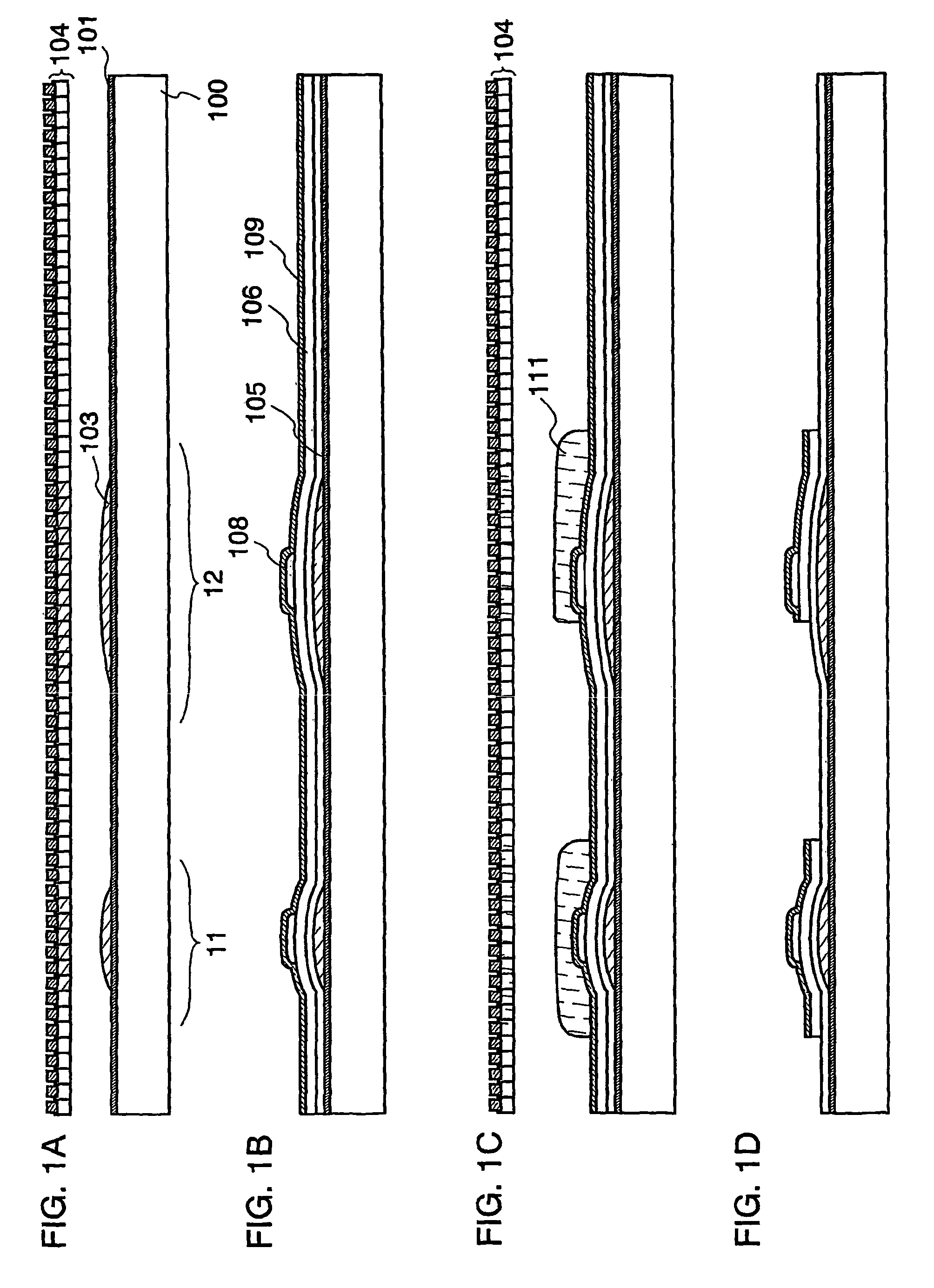
[0059]In this embodiment mode, an example of a method for forming a first and a second thin film transistors.

[0060]First, as shown in FIG. 1A, a substrate 100 having an insulating surface is prepared. For example, a glass substrate such as barium borosilicate glass or alumino borosilicate glass; a quartz substrate; a stainless steel substrate, a bulk semiconductor film; or the like can be used for the substrate 100. Further, a substrate formed of a flexible synthetic resin such as acrylic or plastics typified by polyethylene-terephthalate (PET), a polyethylene naphthalate (PEN), and polyethersulfone (PES) generically has low heat-resistant temperature as compared with a substrate formed of another material. However, such a substrate can be used if it can endure a processing temperature of the fabrication process. In particular, in the case of forming a thin film transistor including an amorphous semiconductor film which does not require a heating process for crystallizing a semicond...

embodiment mode 2

[0124]In this embodiment mode, an example of forming a first and a second thin film transistor with a method different from the above embodiment mode will be described. Specifically, a contact hole provided in an interlayer insulating film is formed in a different manner. The other structure is similar to the above embodiment mode; accordingly, the description will be omitted.

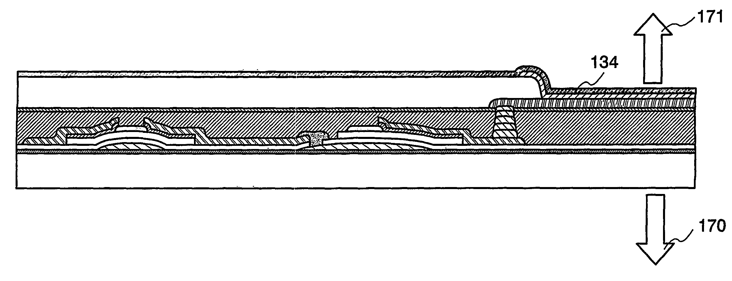
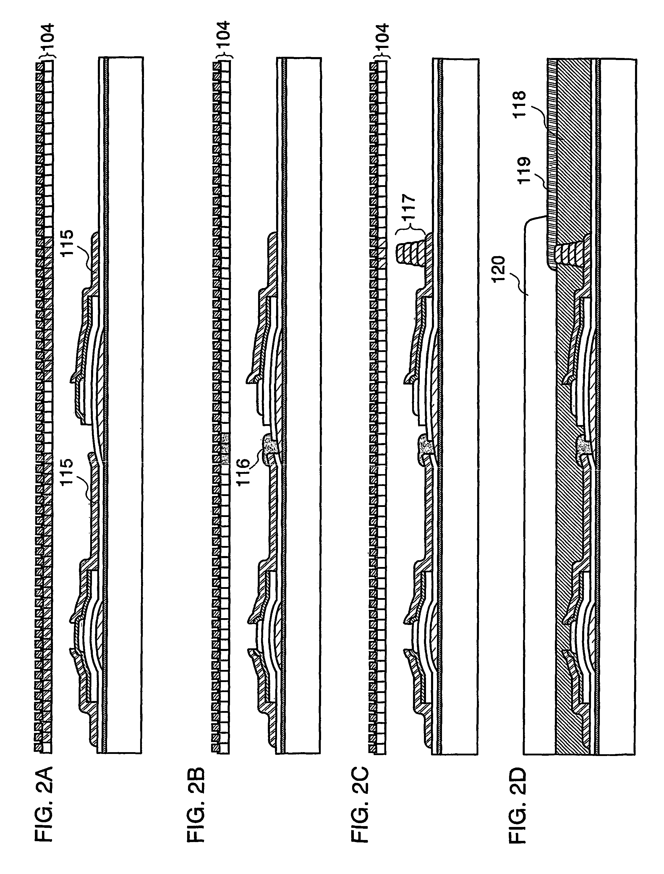
[0125]As shown in FIG. 3A, a first and a second thin film transistors are formed as in the above embodiment mode. In this embodiment mode, an interlayer insulating film 118 is formed so as to cover the first and the second thin film transistors without forming a columnar conductive film.

[0126]Subsequently, a mask is formed over the interlayer insulating film. The mask may be formed by ink-jet or photolithography. In this embodiment mode, the mask is formed by ink-jet. When the mask is formed by ink-jet, a photolithography process can be simplified. In other words, a step of forming a photomask, a light-exposure...

embodiment mode 3

[0132]In this embodiment mode, an example of forming a first and a second thin film transistors with a method different from the above embodiment mode will be described. Specifically, an interlayer insulating film is formed in a different manner. The other structure is similar to the above embodiment mode; accordingly, the description will be omitted.

[0133]As shown in FIG. 4A, a first and a second thin film transistors are formed as in the above embodiment mode, and an interlayer insulating film is formed so as to cover the first and the second thin film transistors. In this embodiment mode, the interlayer insulating film is formed by ink-jet. The interlayer insulating film 125 is formed so as not to overlap one of a source electrode or a drain electrode of the second thin film transistor, which is connected to a pixel electrode. Hereupon, dots containing a material of the insulating film are discharged from nozzles 104 above a region to be provided with the interlayer insulating fi...


PUM

PropertyMeasurementUnit
sizeaaaaaaaaaa
sizeaaaaaaaaaa
sizeaaaaaaaaaa

Abstract

It is an object of the invention to provide a display device which can be manufactured by a simplified manufacturing process by which the efficiency in the use of material is improved. It is a further object of the invention to provide a manufacturing method of the display device. It is another object of the invention to provide a fabrication technology for improving adhesion of a pattern. In view of the above problems, according to the present invention, a pattern is formed by a droplet discharge method. Particularly in the invention, base pretreatment is performed before / after a pattern is formed by a droplet discharge method. As a result of such base pretreatment, adhesion of a pattern can improved, and the pattern may be made finer.

Description

TECHNICAL FIELD[0001]The present invention relates to a display device including an active element such as a transistor formed over a large glass substrate, and further relates to a method for fabricating such a display device.BACKGROUND ART[0002]A display panel including a thin film transistor (hereinafter also referred to as a TFT) over a glass substrate, that is an active matrix drive display panel, has been fabricated by patterning various thin films by means of a light exposure method using a photomask.[0003]As to such a display panel, technologies for effective mass production by which a plurality of display panels can be obtained from one mother glass substrate have been employed. The size of a mother glass has become larger from 300 mm×400 mm of the first generation in the early 1990s to 680 mm×880 mm or 730 mm×920 mm of the fourth generation in 2000. Accordingly, production technology has been improved, so that multiple display panels can be obtained from one mother glass s...

Claims


Application Information

Patent Timeline
Patent Type & Authority Patents(United States)
IPC IPC(8): H01J1/62H01J9/24H01L21/336H01L21/77H01L21/84H01L27/12H01L29/423H01L29/786
CPCH01L27/12H01L27/1292H01L29/66765H01L29/42384H01L29/78696H05B33/10H05B33/14B05D1/26H01L21/02
Inventor YAMAZAKI, SHUNPEIMAEKAWA, SHINJIFUJII, GENKUWABARA, HIDEAKITACHIMURA, YUKO
Owner SEMICON ENERGY LAB CO LTD
Why Eureka
Try Eureka