Pulse phase difference detecting circuit and A/D converter using the same

a phase difference detection and converter technology, applied in pulse automatic control, code conversion, instruments, etc., can solve the problems of delay amount, layout placement, and limitation of design degree of freedom, so as to reduce the sampling time of adc, high speed operation, and high resolution

Active Publication Date: 2011-01-04
RENESAS ELECTRONICS CORP
View PDF6 Cites 12 Cited by
  • Summary
  • Abstract
  • Description
  • Claims
  • Application Information

AI Technical Summary

Benefits of technology

[0022]According to an exemplary embodiment of the present invention, the first delay circuit can be used as a delay unit for securing a delay time, and also can be used as a delay unit for detecting a pulse phase difference. Thus, the sampling time of the ADC is reduced and a high-speed operation can be achieved even at a high bit rate.
[0023]According to an exemplary embodiment of the present invention, it is possible to provide a pulse phase difference detecting circuit having a high resolution and a high operation speed, and an A / D converter using the pulse phase difference detecting circuit.

Problems solved by technology

The flash type and successive approximation type A / D converters, however, require a large number of reference voltages and comparators corresponding to a given resolution, which results in an increase in circuit size and cost of a device.
Additionally, in order to prevent a fluctuation in electrical characteristics of ADCs due to a layout pattern, it is necessary to select a layout pattern from a library of hard macros, resulting in limitation in the degree of freedom of design such as layout placement.
Specifically, an increase in the power supply voltage causes a reduction in the delay amount, and a reduction in the power supply voltage causes an increase in the delay amount.
This makes it difficult to perform a high-speed operation.
When the inverters are used to operate at the voltage close to the threshold voltage Vth, however, the delay amount of the entire delay units increases and the sampling time of the ADC also increases, which makes it difficult to perform a high-speed operation.
In addition, since the transistor operation at the voltage close to the threshold voltage Vth is unstable, the delay variation (jitter) of the inverter increases, which results in a reduction in conversion accuracy of the ADC.
The present inventor has found a problem that, when a plurality of delay units for securing a delay time are connected in series at the previous stage of a pulse phase difference detecting circuit, the sampling time of an ADC increases, and a high-speed operation becomes increasingly difficult as the bit rate becomes higher.

Method used


Image

  • Pulse phase difference detecting circuit and A/D converter using the same
  • Pulse phase difference detecting circuit and A/D converter using the same
  • Pulse phase difference detecting circuit and A/D converter using the same

Examples


first exemplary embodiment

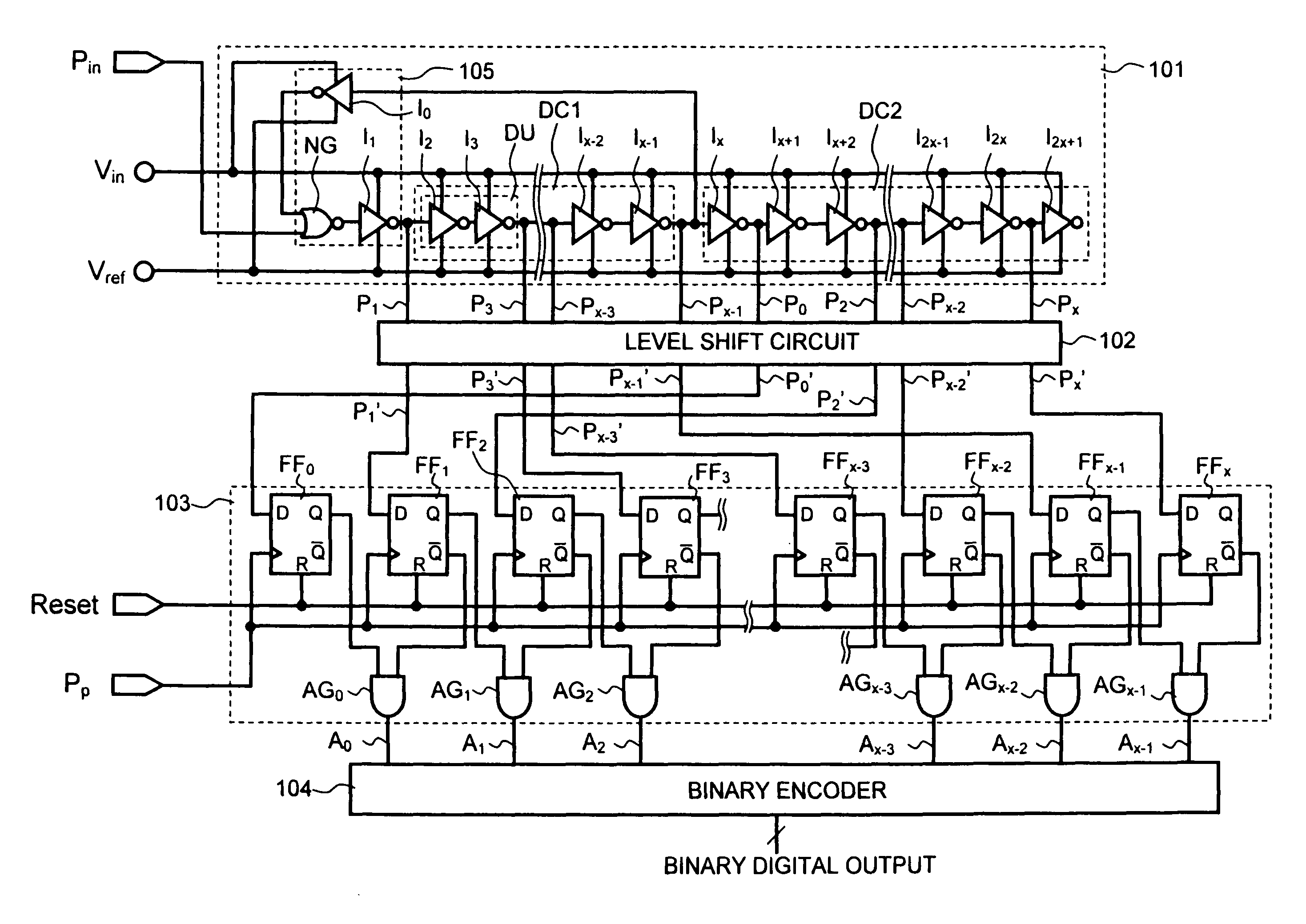
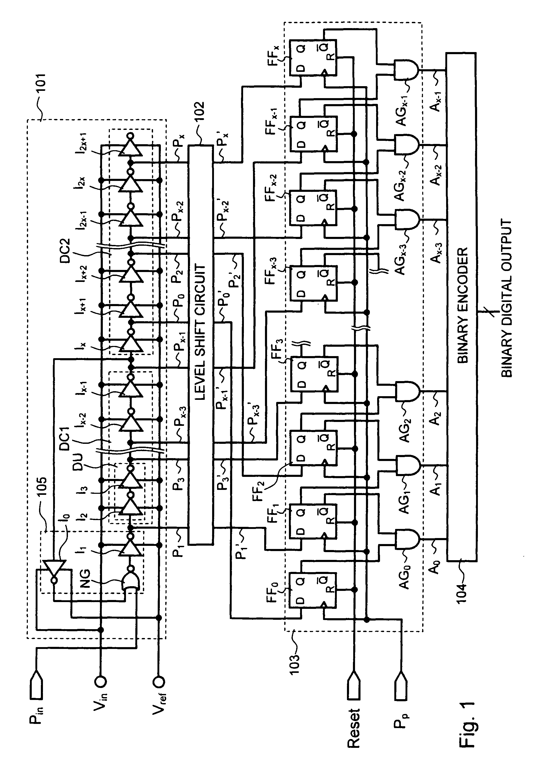
[0035]Exemplary embodiments of the present invention will be described below with reference to the accompanying drawings. FIG. 1 is a circuit diagram showing an ADC using a pulse phase difference detecting circuit according to a first exemplary embodiment of the present invention. As shown in FIG. 1, the ADC according to the first exemplary embodiment includes a pulse phase difference detecting circuit 101, a level shift circuit 102, a pulse edge detecting circuit 103, and a binary encoder 104.

[0036]Referring to FIG. 1, the pulse phase difference detecting circuit 101 includes a NOR gate NG and (2x+2) number of inverters I0, I1, I2, I3, . . . , Ix−2, Ix−1, Ix, Ix+1, Ix+2, I2x−1, I2x, and I2x+1. Inverters I4 to Ix−3 and inverters Ix+3 to I2x−2 are omitted in FIG. 1. In this case, assuming that the ADC has a resolution of n bits, “x” is expressed as x=2n. Each of the inverters operates at a voltage between a reference voltage Vref and an input voltage Vin. For example, when the refere...

second exemplary embodiment

[0057]Next, another exemplary embodiment of the present invention will be described. FIG. 4 is a circuit diagram showing an ADC according to a second exemplary embodiment of the present invention. Components identical with those of the first exemplary embodiment are denoted by the same reference symbols, and description thereof is omitted as appropriate. As shown in FIG. 4, the ADC according to the second exemplary embodiment includes a pulse edge detecting circuit 203 including NOR gates in replace of the AND gates shown in FIG. 1. The other components are similar to those of the first exemplary embodiment.

[0058]A NOR gate NG0 receives a signal output from the output terminal Q of the D flip-flop FF0, and a signal output from the output terminal Q of the D flip-flop FF1. A NOR gate NG1 receives a signal obtained by inverting a signal output from the output terminal Q of the D flip-flop FF1 by an inverter, and a signal output from the output terminal Q of the D flip-flop FF2. Likewi...

third exemplary embodiment

[0061]Next, still another exemplary embodiment of the present invention will be described. FIG. 5 is a circuit diagram showing a pulse phase difference detecting circuit according to a third exemplary embodiment of the present invention. FIG. 6 is a block diagram showing an ADC using the pulse phase difference detecting circuit according to the third exemplary embodiment. Components identical with those of the first exemplary embodiment are denoted by the same reference symbols, and description thereof is omitted as appropriate.

[0062]When the inverters constituting the pulse phase difference detecting circuit 101 according to the first and second exemplary embodiments are used to operate at a voltage close to a threshold voltage Vth of a CMOS transistor, a delay variation due to a change in voltage increases. This increases the total delay amount of delay units and the sampling time of the ADC, which makes it difficult to perform a high-speed operation. In addition, transistor opera...


PUM


Abstract

Provided is a pulse phase difference detecting circuit including: a first delay circuit that receives a first pulse signal to output a signal obtained by delaying the first pulse signal as a second pulse signal and includes multiple serially-connected delay units having the same delay amount; a second delay circuit that receives the second pulse signal and includes multiple serially-connected delay units having the delay amount; a first delay adjustment circuit that adjusts a delay amount with respect to the second pulse signal and outputs the adjusted second pulse signal back to the first delay circuit as a third pulse signal; and a pulse arrival position detecting circuit that detects a pulse arrival position of the first pulse signal based on outputs of the delay units of the first and second delay circuits that are transmitted as the third and second pulse signals, respectively.

Description

BACKGROUND[0001]1. Field of the Invention[0002]The present invention relates to a pulse phase difference detecting circuit and an A / D converter using the same.[0003]2. Description of Related Art[0004]In general, examples of A / D converters (ADCs: analog-to-digital converters) for converting analog signals into digital signals at high speed include a flash type A / D converter and a successive approximation type A / D converter. The flash type and successive approximation type A / D converters, however, require a large number of reference voltages and comparators corresponding to a given resolution, which results in an increase in circuit size and cost of a device. In order to improve the accuracy of each of the reference voltages and comparators, semiconductor processes and devices with excellent analog characteristics are required. Additionally, in order to prevent a fluctuation in electrical characteristics of ADCs due to a layout pattern, it is necessary to select a layout pattern from ...

Claims


Application Information

Patent Timeline
Patent Type & Authority Patents(United States)
IPC IPC(8): H03M1/60
CPCG01R25/005H03M1/502
Inventor OBA, HIROYUKI
Owner RENESAS ELECTRONICS CORP
Why Eureka
Try Eureka