Method for production of thin semiconductor solar cells and integrated circuits

a technology of solar cells and solar cells, applied in the field of production of thin semiconductor solar cells and integrated circuits, can solve the problems of high efficiency, high cost of monocrystalline silicon wafers, and long dwell time, and achieve the effect of high mechanical strength and high temperature capability of ceramics

Inactive Publication Date: 2011-01-11
VU DUY PHACH +1
View PDF2 Cites 0 Cited by
  • Summary
  • Abstract
  • Description
  • Claims
  • Application Information

AI Technical Summary

Benefits of technology

[0017]The present invention describes a method that combines two processes, zone-melting recrystallization (ZMR) and circuit transfer, to fabricate a thin crystalline silicon layer in which very low-cost and highly efficient silicon solar cells and / or integrated circuits can be produced.
[0021]The solar cells fabricated in the recrystallized silicon can achieve the high efficiency and reliability of crystalline silicon while using one-hundredth of the amount of silicon used if the same cells were made in a bulk silicon wafer.
[0023]The ceramic substrate released by the lift-off is unaffected by the ZMR process and the device fabrication process and can be re-used repeatedly. This re-usability results from the high mechanical strength and very high temperature capability of ceramics.

Problems solved by technology

Although monocrystalline silicon solar cells have the highest efficiency, the high efficiency comes with the high cost of the monocrystalline silicon wafers.
With the graphite strip or the halogen lamp, the long dwell time can only produce material in which devices / circuits can be processed afterward.

Method used


Image

  • Method for production of thin semiconductor solar cells and integrated circuits
  • Method for production of thin semiconductor solar cells and integrated circuits
  • Method for production of thin semiconductor solar cells and integrated circuits

Examples


Embodiment Construction

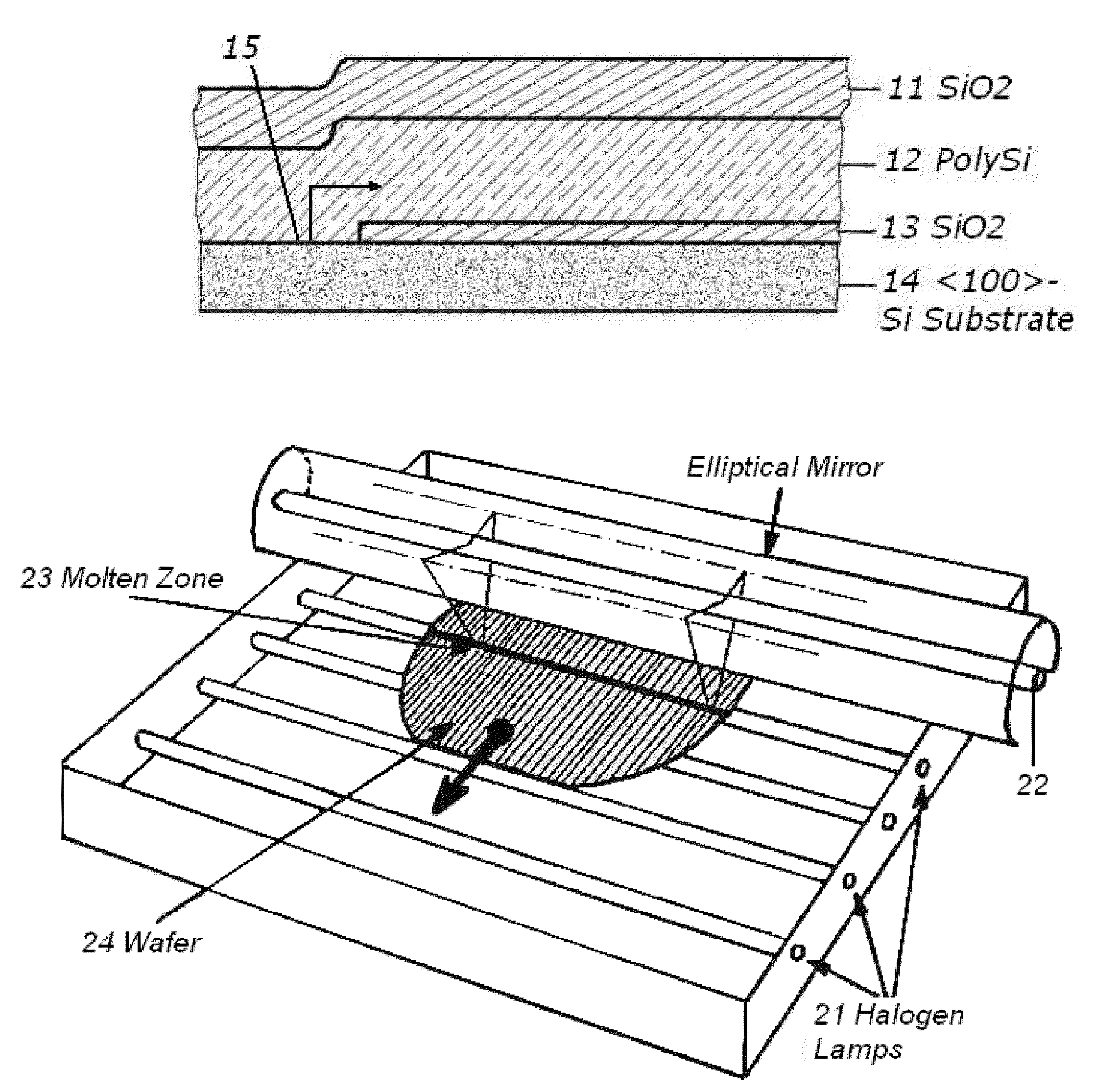
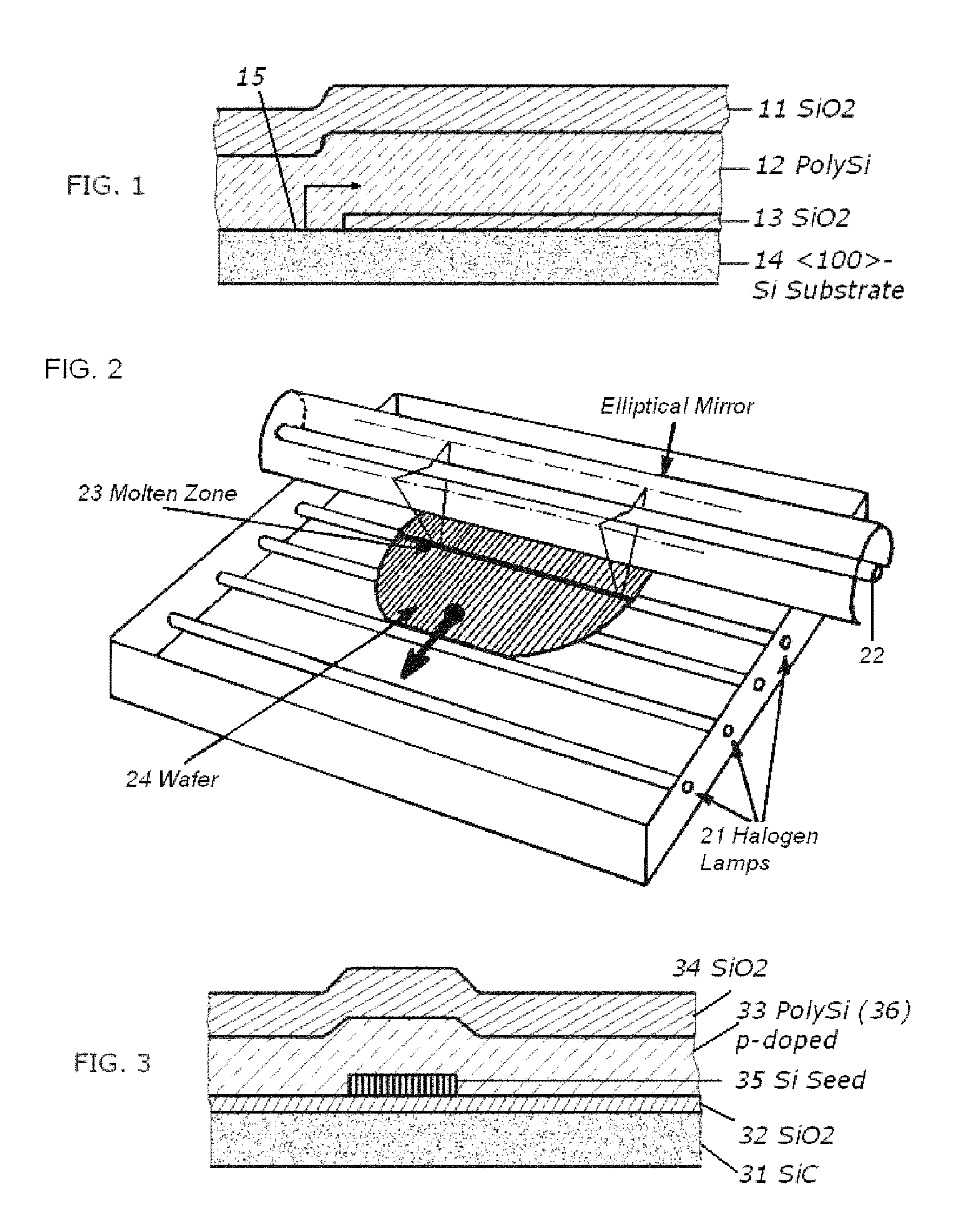
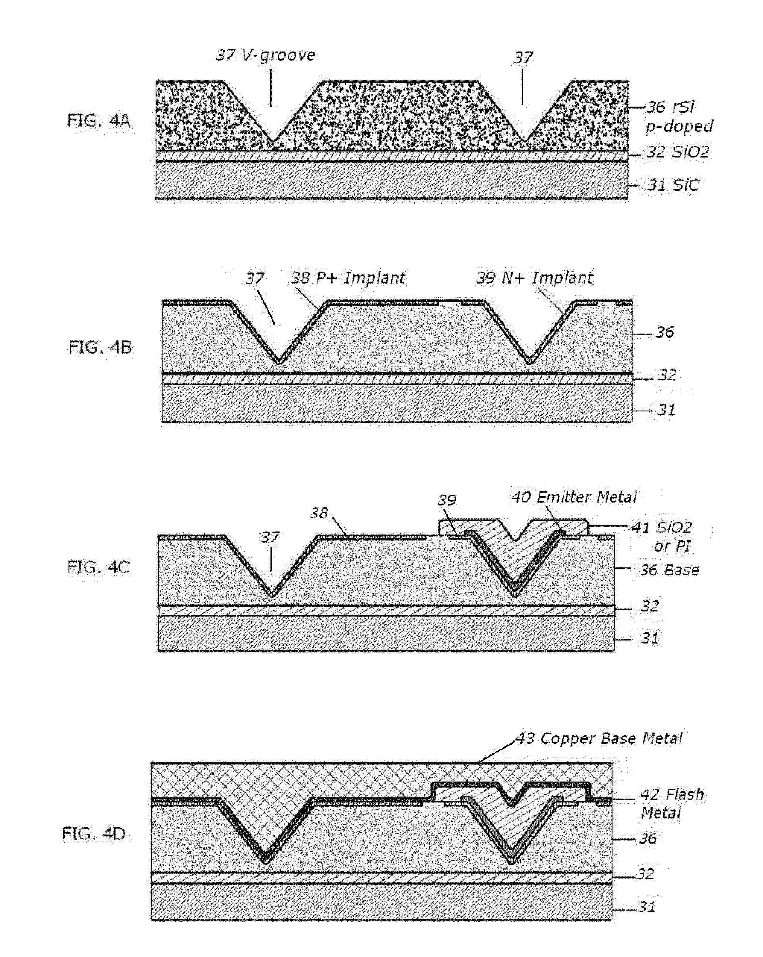
[0030]Embodiments of the present invention will now be described more fully with reference to the accompanying drawings, in which the embodiments are shown. The present invention may, however, be embodied in many different forms and should not be construed as being limited to the embodiments set forth herein; rather, the embodiments are provided so that this disclosure will be thorough and complete, and will fully convey the concept of the invention to one skilled in the art. In the drawings, the dimensions and regions are exaggerated for clarity. Like reference numerals in the drawings denote like elements, and thus, their description will not be repeated.

[0031]Accordingly, while embodiments of the invention are capable of various modifications and alternative forms, only the embodiments thereof are shown by way of example in the drawings and will herein be described in detail. It should be understood, however, that there is no intent to limit embodiments of the invention to the pa...


PUM

PropertyMeasurementUnit
thicknessaaaaaaaaaa
temperatureaaaaaaaaaa

Abstract

The invention relates to the formation of thin-film crystalline silicon using a zone-melting recrystallization process in which the substrate is a ceramic material. Integrated circuits and solar cells are fabricated in the recrystallized silicon thin film and lifted off the substrate. Following lift-off, these circuits and devices are self-sustained, lightweight and flexible and the released ceramic substrate can be reused making the device fabrication process cost effective.

Description

PRIORITY STATEMENT[0001]The present application claims benefit from the U.S. provisional application No. 61 / 080,041 filed on Jul. 11, 2008, the disclosure of which is incorporated herein in its entirety by reference.BACKGROUND OF THE INVENTION[0002]1. Field[0003]A solar cell is a device that converts sunlight into electricity by the photovoltaic effect. The solar cell consists of a p-n junction fabricated in a single-crystal semiconductor material, such as silicon, germanium or gallium-arsenide.[0004]2. Description of the Related Art[0005]Currently, silicon cells account for over 90% of the solar cell fabricated in the world (see L. L. Kazmerski, “Solar photovoltaics R&D at the tipping point: A 2005 technology overview”, J. of Electron Spectroscopy and Related Phenomena, 150 (2006), 105-135).[0006]Silicon solar cells can be divided into three groups, depending on the quality of the material: (1) monocrystalline silicon solar cells, which can have efficiencies approaching the theoret...

Claims


Application Information

Patent Timeline
Patent Type & Authority Patents(United States)
IPC IPC(8): H01L21/00
CPCH01L21/02378H01L21/0245H01L21/02488H01L21/02502H01L21/02532H01L21/02609H01L21/02667H01L31/022425H01L31/035281H01L31/03529H01L31/03921H01L31/068H01L31/1872Y02E10/547H01L31/022441H01L31/0682Y02P70/50
Inventor VU, DUY-PHACHVU, QUOC-BAO
Owner VU DUY PHACH
Why Eureka
Try Eureka