Surface emitting laser

a laser and surface technology, applied in the field of surface emitting lasers, can solve the problems of increasing voltage, reducing power efficiency, and displaying higher electric resistance, and achieve the effect of lowering the electric resistance originating

Inactive Publication Date: 2011-01-11
CANON KK
View PDF25 Cites 31 Cited by
  • Summary
  • Abstract
  • Description
  • Claims
  • Application Information

AI Technical Summary

Benefits of technology

[0020]In view of the above described problem, an object of the present invention is to provide a surface emitting laser using a photonic crystal structure, which lowers electric resistance originating in a cladding layer and also can inhibit light from being absorbed by an electrode.
[0023]The hole constituting the photonic crystal structure is set so as to have a depth of 100 nm or more, which can inhibit light from leaking to the electrode. As a result, a cladding layer to be provided between the photonic crystal structure and the electrode can be made thin or can be eliminated, while inhibiting the light from being absorbed by the electrode. As a result, the electrode and the active layer can be closely arranged to lower the electric resistance.

Problems solved by technology

However, such a thick cladding layer causes the increase of electric resistance, consequently causes the increase of voltage and the degradation of power efficiency, and gives an influence on device characteristics.
However, such a ternary solid solution crystal has a problem of showing higher electric resistance than a binary crystal.
However, when the thickness of the p-type cladding layer is simply reduced, the distance between an electrode and the active layer is narrowed, which causes a problem that the electrode absorbs the horizontally resonating light.
In other words, when the p-type cladding layer is thinned so as to lower the electric resistance, the p-type cladding layer cannot inhibit light from leaking, and the light is absorbed by the electrode, which may reduce emission efficiency.

Method used


Image

  • Surface emitting laser
  • Surface emitting laser
  • Surface emitting laser

Examples


exemplary embodiment 1

[0062]In Exemplary embodiment 1, a photonic-crystal surface emitting laser to which the present invention is applied will be described.

[0063]FIG. 4 illustrates a schematic sectional view for describing a structure of a photonic-crystal surface emitting laser to which the present invention is applied.

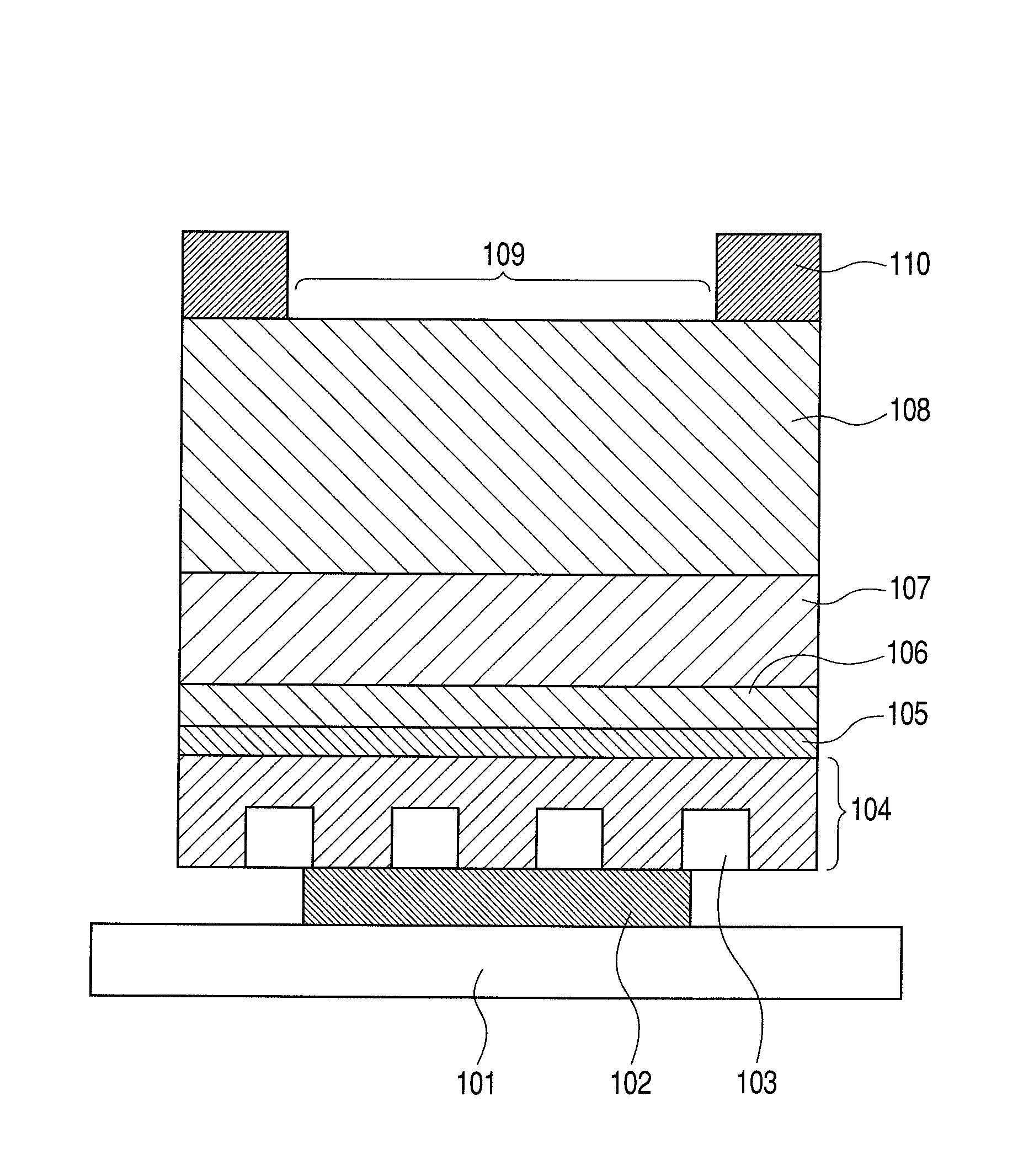
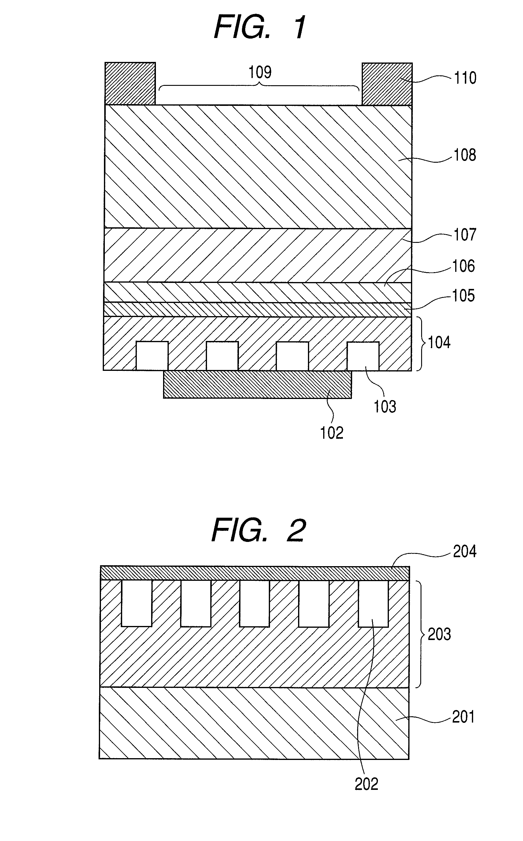
[0064]In FIG. 4, the same element as that illustrated in FIG. 1 is designated by the same reference numeral. An SiC substrate 101 has an electrode pattern on its surface.

[0065]The surface emitting laser of the present embodiment is constituted by a plurality of semiconductor layers including a photonic crystal structure 103 laminated on a GaN substrate 108, and emits a laser beam having a wavelength λ from the rear face side with respect to the laminated face of the semiconductor layers.

[0066]Specifically, a p-type electrode 102 is formed so as to contact with a p-GaN layer 104 (photonic crystal layer) in which the photonic crystal structure 103 has been produced up to the middle of the ...

exemplary embodiment 2

[0088]In Exemplary embodiment 2, a structure example including a multilayer reflector in the photonic crystal layer will now be described.

[0089]In the present exemplary embodiment, the multilayer reflector formed of semiconductors is provided in the photonic crystal layer, and accordingly can enhance the light extraction efficiency.

[0090]FIG. 6 illustrates a schematic sectional view for describing a structure of a surface emitting laser in the present exemplary embodiment.

[0091]In FIG. 6, the same element as that illustrated in FIG. 1 is designated by the same reference numeral. The structure of the present exemplary embodiment has a semiconductor DBR 605 formed of laminated mirrors of a pair of two types of semiconductor layers 602 and 603 having mutually different refractive indices in the photonic crystal layer, which is a different point.

[0092]In the present exemplary embodiment, the first semiconductor layer 602 of the semiconductor DBR 605 is made from the same material as tha...

exemplary embodiment 3

[0098]In Exemplary embodiment 3, a structure example will now be described in which a multilayer reflector formed of semiconductors is provided in a region on the laser beam emission side, which region is farther than the p-type semiconductor layer in the above described laminated structure.

[0099]A photonic-crystal surface emitting laser in the present exemplary embodiment is structured so that a DBR is formed in the n-side, and so that the Q-value and extraction efficiency can be controlled.

[0100]FIG. 7 illustrates a schematic sectional view for describing a structure of a photonic-crystal surface emitting laser according to the present exemplary embodiment.

[0101]In FIG. 7, the same element as that illustrated in FIG. 1 is designated by the same reference numeral.

[0102]The present exemplary embodiment has basically the same structure as in Exemplary embodiment 1, but is different from Exemplary embodiment 1 in that a DBR 703 is provided on an n-cladding layer.

[0103]In the present e...


PUM


Abstract

A surface emitting laser which oscillates at a wavelength λ of a blue band, including a photonic crystal layer including a photonic crystal structure, an active layer provided on one surface of the photonic crystal layer, and an electrode provided on the other surface of the photonic crystal layer for injecting electric current into the active layer. The photonic crystal structure has a thickness of 100 nm or more. A laser beam is emitted toward a direction opposite to a side of the photonic crystal layer on which the electrode is provided.

Description

BACKGROUND OF THE INVENTION[0001]1. Field of the Invention[0002]The present invention relates to a surface emitting laser, and particularly relates to a surface emitting laser of a blue band using a photonic crystal.[0003]2. Description of the Related Art[0004]In recent years, a surface emitting laser which can emit light in a direction vertical to a substrate has received attention.[0005]For instance, a vertical resonator type surface emitting laser (VCSEL: Vertical Cavity Surface Emitting Laser) is a laser which emits a laser beam in a direction vertical to a substrate, and has an advantage of being easily two-dimensionally arrayed in high density.[0006]Japanese Patent Application Laid-Open No. 2006-165309 proposes a surface emitting laser provided with a photonic crystal structure.[0007]FIG. 10 illustrates a structure of the surface emitting laser using the photonic crystal structure disclosed in Japanese Patent Application Laid-Open No. 2006-165309.[0008]This surface emitting la...

Claims


Application Information

Patent Timeline
Patent Type & Authority Patents(United States)
IPC IPC(8): H01S3/08
CPCH01S5/187H01S5/32341H01S5/105H01S5/3211H01S5/11
Inventor UCHIDA, TAKESHINAGATOMO, YASUHIROHORI, YUICHIROIKUTA, MITSUHIRO
Owner CANON KK
Why Eureka
Try Eureka