Light-emitting device

a light-emitting device and light-emitting technology, applied in the direction of organic semiconductor devices, identification means, instruments, etc., can solve the problems of not reaching the technical level of developing applied technology for tft using a conventional oxide-semiconductor thin film, and the difficulty of directly forming silicon thin film on a resin substrate with low heat resistan

Active Publication Date: 2011-01-18
CANON KK +2
View PDF31 Cites 142 Cited by
  • Summary
  • Abstract
  • Description
  • Claims
  • Application Information

AI Technical Summary

Benefits of technology

[0039]Consequently, the present inventors found that a TFT prepared by using an amorphous oxide containing electronic carriers with a concentration of less than 1×10¹⁸ / cm3 as an active layer of a field effect transistor can show desired characteristics, and can be applied to a flat panel display such as a light-emitting device.

Problems solved by technology

However, because a thermal process in a comparatively high temperature is necessary to manufacture a transistor with the use of the above described silicon thin film, it is difficult to directly form the silicon thin film on a resin substrate with low heat resistance.
However, the TFT using a conventional oxide-semiconductor thin film does not reach a technical level of developing the applied technology, probably because of not having attained sufficient characteristics such as in a TFT using silicon.

Method used


Image

  • Light-emitting device
  • Light-emitting device
  • Light-emitting device

Examples


first embodiment

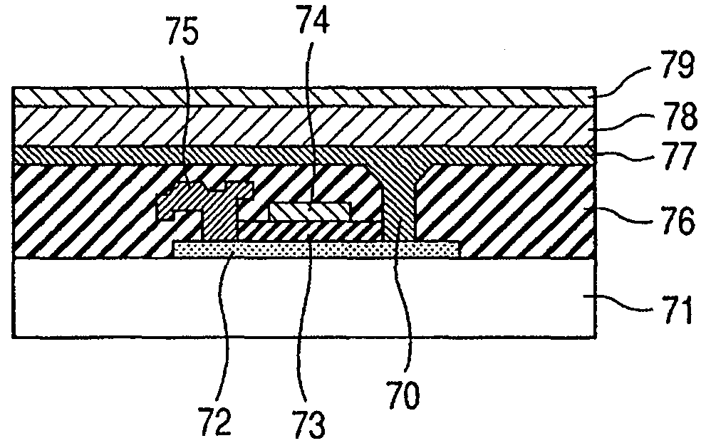
[0088]A source electrode 75 and a drain electrode 70 are directly connected with an active layer 72, and the current passing through the active layer 72 is controlled by a gate electrode 74 through a gate insulation film 73.

[0089]An organic EL layer 78 of a light-emitting layer is connected with a drain electrode 70, through a bottom electrode 77 and a wire in a contact hole. An interlayer insulation layer 76 exists between the bottom electrode 77 and a TFT section to electrically insulate them. The interlayer insulation layer 76 does not necessarily need to be a single layer, but generally consists of insulation layers arranged on the gate insulation film and on the upper part of the gate electrode, and the general interlayer insulation layer for a flattening purpose.

[0090]A counter electrode 79 exists on the upper part of the organic EL layer 78, and applies voltage to the organic EL layer 78 to make it emit light when a TFT is turned ON.

[0091]Here, a drain electrode 70 is electri...

second embodiment

[0108]In FIG. 9, reference numeral 91 denotes a substrate, reference numeral 92 an active layer made of a semiconductor material peculiar to the present invention, reference numeral 93 a gate insulation film, reference numeral 94 a gate electrode, reference numeral 95 a source electrode, reference numeral 96 an insulation layer, and reference numeral 97 a bottom electrode. The bottom electrode 97 is layered on a drain electrode or is identical to the drain electrode, in other words, is the drain electrode in itself. Reference numeral 98 denotes an organic EL layer, and reference numeral 99 a counter electrode.

[0109]The present embodiment has basically the same type of configuration in the first embodiment in which a part of a bottom electrode contacts with a drain electrode through wiring, but has a different configuration in which the drain electrode and a light-emitting layer are layered on the same overlapping area when viewed from the position above a substrate 91, and the botto...

third embodiment

[0118]In FIG. 8, reference numeral 81 denotes a transistor for driving an organic EL layer 84, which passes a current to a light-emitting element that has the organic EL layer 84 and a pair of electrodes sandwiching the organic EL layer 84. Reference numeral 82 is a transistor 2 for selecting a picture element, which supplies a picture signal for determining a current to be passed to the light-emitting element, to a gate of the transistor 81.

[0119]In addition, a condenser 83 is placed in order to hold a selected condition, stores electrical charges between a common electrode wire 87 and a source electrode part of the transistor 2, and retains the signal of the gate of the transistor 1. The picture element is selected and determined by a scan electrode wire 85 and a signal electrode wire 86.

[0120]The configuration will be now more specifically described.

[0121]At the same time when a row selection signal is applied to a gate electrode from a driver circuit (not shown) through a scan e...


PUM


Abstract

An object of the present invention is to provide a new light-emitting device with the use of an amorphous oxide. The light-emitting device has a light-emitting layer existing between first and second electrodes and a field effect transistor, of which the active layer is an amorphous.

Description

BACKGROUND OF THE INVENTION[0001]1. Field of the Invention[0002]The present invention relates to a light-emitting device using an oxide, and particularly using an organic EL element and an inorganic EL element. The light-emitting device according to the present invention also relates to a top emission type or a bottom emission type.[0003]2. Related Background Art[0004]In recent years, a flat panel display (FPD) is in practical use as a result of the progress of technologies relating to a liquid crystal and electroluminescence (EL). The FPD is driven by an active matrix circuit consisting of a field effect thin film transistor (TFT) using an amorphous silicon thin film or a polycrystalline silicon thin film provided on a glass substrate as an active layer.[0005]On the other hand, an attempt has been made to use a lightweight and flexible resin substrate in place of the glass substrate, in quest of further improvement in thinning, slimming and breakage resistance of an FPD. However, b...

Claims


Application Information

Patent Timeline
Patent Type & Authority Patents(United States)
IPC IPC(8): H01L31/20B41J2/44B41J2/45B41J2/455G09F9/30H01L27/32H01L29/786H01L51/50H05B33/10
CPCG03G5/08G03G5/144H01L27/1214H01L29/04H01L29/7869H01L27/3248H01L27/3262H01L2251/5315H01L29/66969H01L29/78693H01L27/1225H10K59/123H10K59/1213H10K2102/3026H01L21/02592H01L29/1025H01L29/41725
Inventor DEN, TOHRUIWASAKI, TATSUYAHOSONO, HIDEOKAMIYA, TOSHIONOMURA, KENJI
Owner CANON KK
Why Eureka
Try Eureka