Silicon/germanium oxide particle inks, inkjet printing and processes for doping semiconductor substrates

Inactive Publication Date: 2011-02-22
NANOGRAM
View PDF30 Cites 9 Cited by
  • Summary
  • Abstract
  • Description
  • Claims
  • Application Information

AI Technical Summary

Problems solved by technology

With increasing costs and undesirable environmental effects from the use of fossil fuels and other non-renewable energy sources, there are growing demands for alternative forms of energy.

Method used


Image

  • Silicon/germanium oxide particle inks, inkjet printing and processes for doping semiconductor substrates
  • Silicon/germanium oxide particle inks, inkjet printing and processes for doping semiconductor substrates
  • Silicon/germanium oxide particle inks, inkjet printing and processes for doping semiconductor substrates

Examples


example 1

SiO2 Dispersion in Methyl Ethyl Ketone (MEK)

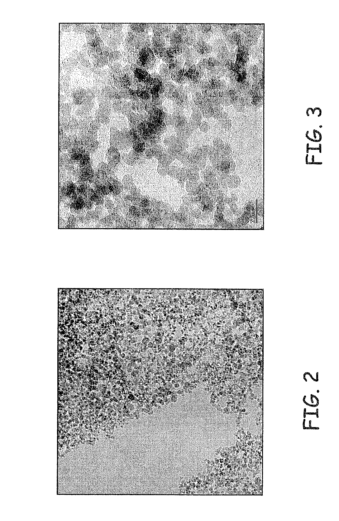
[0099]This example demonstrates the dispersion and surface modification of silica particles synthesized using laser pyrolysis.

[0100]SiO2 was produced by laser pyrolysis aerosol) with Tetraethoxylsilane (TEOS) as the silicon precursor. The silicon precursor was delivered with as an aerosol with a mixture of ethylene, oxygen and an inert gas serving as the carrier gas. The apparatus was similar to the apparatus in FIGS. 6-8 of U.S. Pat. No. 6,849,334 to Home et al., entitled “Optical Materials and Optical Devices,” incorporated herein by reference. The SiO2 particles had a primary particle size as determined using a transmission electron micrograph of 10-20 nm. Transmission electron micrographs at two magnifications are shown in FIGS. 2 and 3, respectively, for a representative SiO2 nanoparticle sample made from TEOS using laser pyrolysis.

[0101]SiO2 powder (13.6 g, with a BET surface area>236.5 m2 / g) was added to methylethylketone (MEK) to m...

example 2

SiO2 Dispersion in Isopropanol

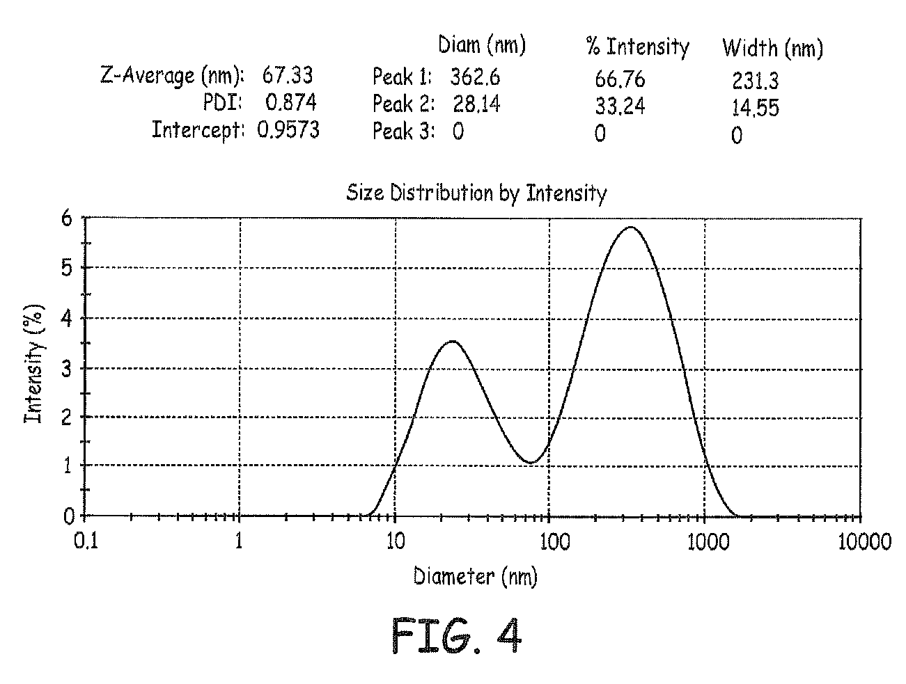
[0102]This example demonstrated the dispersion of SiO2 nanoparticles in isopropanol as an alternative dispersing liquid. The SiO2 nanoparticles for this example had the same property as the nanoparticles in Example 1.

[0103]SiO2 powder (1.0 g, with a BET surface area 214.0 m2 / g) was added to isopropanol to make a 1% wt mixture. The mixture was sonicated in a bath sonicator for 1-4 hours. Then, N-(2-aminoethyl)-3-aminopropyltrimethoxysilane (0.32 g-1.94 g, Gelest, Inc.) was added to the dispersion and continue sonication for 1-7 hr at a temperature of 25° C.-60° C. The resultant secondary particles sizes were evaluated with dynamic light scattering (DLS) using a Malvern ZetaSizer™ instrument. The distribution of the size of the particles revealed from DLS measurement is shown in FIG. 5 where the particles had an average secondary particle size of about 99.7 nm. SiO2 particles therefore form good dispersion in IPA at 1% wt after modification with N-(2-amin...


PUM

PropertyMeasurementUnit
volume-average particle sizeaaaaaaaaaa

Abstract

Highly uniform silica nanoparticles can be formed into stable dispersions with a desirable small secondary particle size. The silican particles can be surface modified to form the dispersions. The silica nanoparticles can be doped to change the particle properties and / or to provide dopant for subsequent transfer to other materials. The dispersions can be printed as an ink for appropriate applications. The dispersions can be used to selectively dope semiconductor materials such as for the formation of photovoltaic cells or for the formation of printed electronic circuits.

Description

CROSS REFERENCE TO RELATED APPLICATIONS[0001]This application claims priority to U.S. provisional patent application Ser. No. 60 / 878,239 filed on Jan. 3, 2007 to Hieslmair et al., entitled “Doped Dispersions and Processes for Doping Semiconductor Substrates,” incorporated herein by reference.FIELD OF THE INVENTION[0002]The invention relates to dispersions / inks of silica / germania particles, such as doped silica particles. The invention further relates to inks that are suitable for ink jet printing. Additionally, the invention relates to the use of doped silica / germania particles for the doping of semiconductor substrates, such as through the drive in of dopants with heat and / or light from a silica / germania deposit formed through inkjet printing onto the semiconductor surface.BACKGROUND OF THE INVENTION[0003]The formation of semiconductor devices generally involves the formation of doped regions in which the dopants alter the electrical conduction properties or other desired propertie...

Claims


Application Information

Patent Timeline
Patent Type & Authority Patents(United States)
IPC IPC(8): H01L21/00H01L29/06
CPCB82Y30/00C09C1/3081C09D11/30C09D11/38H01L21/02532H01L21/02601H01L21/02628H01L31/1804H05K1/097Y10T428/24909C01P2002/72C01P2004/54C01P2004/62C01P2004/64C01P2006/12Y10S977/773Y10S438/933Y10S977/786Y10S977/774Y02E10/547Y02P70/521Y10T428/12674C01P2002/52Y02P70/50C09C3/12B82B3/00H01L21/3115B82Y40/00
Inventor HIESLMAIR, HENRYCHIRUVOLU, SHIVKUMARDU, HUI
Owner NANOGRAM
Why Eureka
Try Eureka