Field effect transistor

a field effect transistor and transistor technology, applied in transistors, semiconductor devices, electrical devices, etc., can solve the problems of difficult to form a satisfactory interface between the gate insulating layer and the channel layer and achieve satisfactory transistor characteristics and operation stability. , the effect of generating hysteresis

Inactive Publication Date: 2011-03-15
CANON KK
View PDF27 Cites 59 Cited by
  • Summary
  • Abstract
  • Description
  • Claims
  • Application Information

AI Technical Summary

Benefits of technology

[0030]Also, the satisfactory transistor characteristics include a high field-effect mobility and being normally off.
[0033]When the TFT is used in, for example, a pixel circuit of a display, generation of hysteresis creates variations in operation of an organic LED, liquid crystal, or the like to be driven, which ultimately leads to degraded image quality of the display. Accordingly, an object of the present invention is to materialize a thin film transistor which attains both satisfactory transistor characteristics and operation stability.
[0034]Another object of the present invention is to decrease the above-mentioned hysteresis and to improve drive stability of a thin film transistor using an oxide as a channel layer by modifying an oxide material used for a gate insulating layer.

Problems solved by technology

However, with those gate insulating layers, it is difficult to attain both satisfactory transistor characteristics and operation stability.
One reason is thought to be that, with those gate insulating layers, it is difficult to form a satisfactory interface between the gate insulating layer and the channel layer.

Method used


Image

  • Field effect transistor
  • Field effect transistor
  • Field effect transistor

Examples


example 1

Amorphous Ga2O3 Insulating Layer

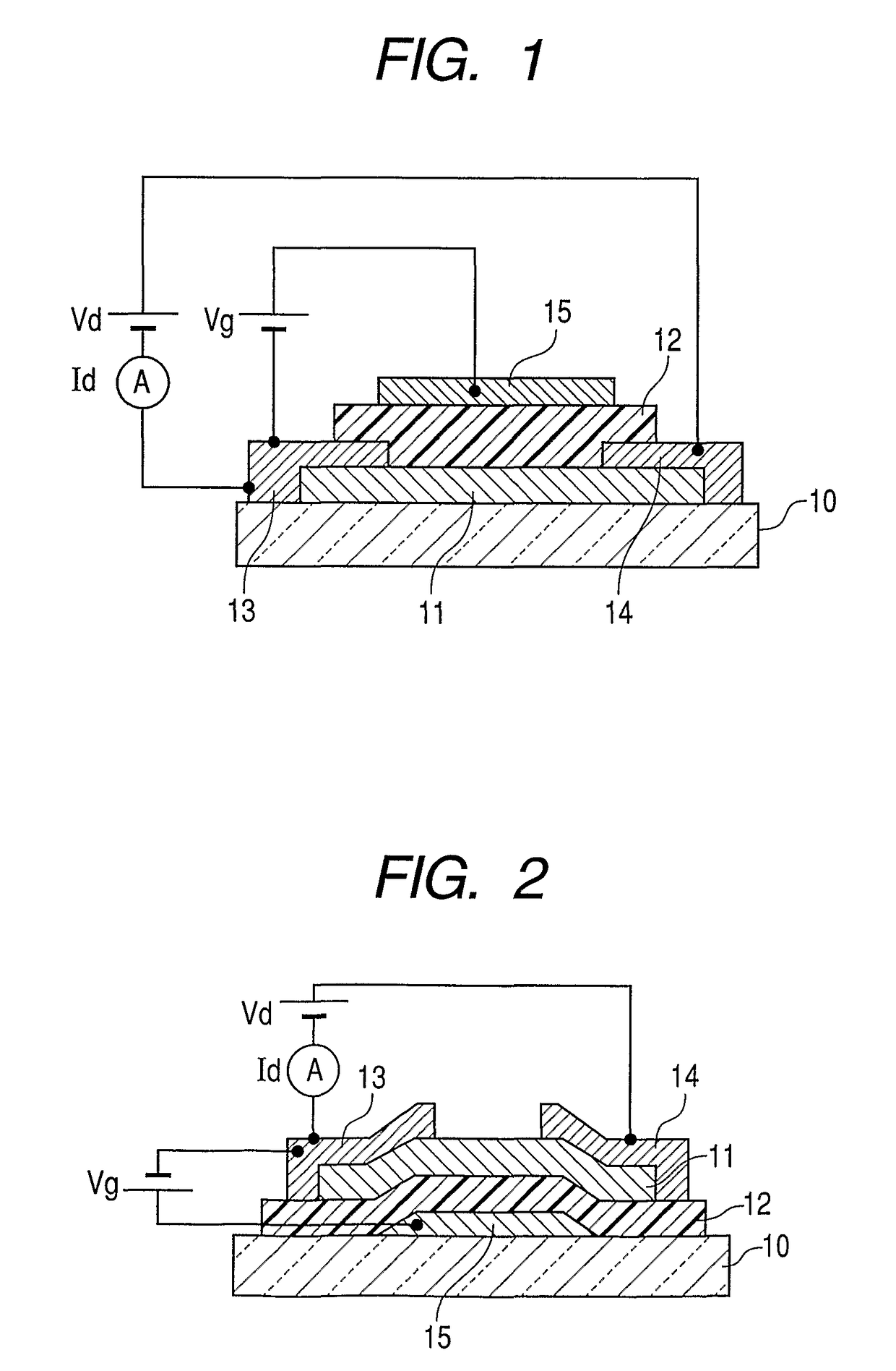
[0140]In this example, the top-gate type TFT device illustrated in FIG. 1 was manufactured.

[0141]The TFT device had a channel layer formed of an In—Ga—Zn—O-based amorphous oxide and a gate insulating layer formed of amorphous Ga2O3.

[0142]First, an amorphous oxide film as the channel layer 11 was formed on the glass substrate 10 (Corning #1737).

[0143]In this example, the In—Zn—Ga—O-based amorphous oxide film was formed by radio-frequency sputtering in a mixed gas atmosphere of argon gas and oxygen gas.

[0144]A sputtering apparatus as illustrated in FIG. 8 was used.

[0145]In FIG. 8, reference numerals 51, 52, 53, 54, 55, 56, 57, and 58 denote a sample, a target, a vacuum pump, a vacuum gauge, a substrate holding means, gas flow-rate control means provided for the respective gas introduction systems, a pressure-control means, and a film-forming chamber, respectively.

[0146]There were provided three gas introduction systems for argon, oxygen, and a mixed gas...

example 2

Amorphous Ga—In—O Insulating Layer

[0182]In this example, a top gate type TFT device illustrated in FIG. 1 was manufactured.

[0183]An amorphous oxide containing Ga as the main component and containing In as the sub component was used as the gate insulating layer.

[0184]First, an In—Zn—Ga—O-based amorphous oxide film was deposited on a glass substrate (Corning #1737) by a PLD method using a KrF excimer laser.

[0185]The In—Zn—Ga—O-based amorphous oxide film was deposited with a polycrystalline sintered material having a composition of InGaO3 (ZnO) 4 used as the target. The oxygen partial pressure when the film was formed was 6 Pa.

[0186]It is to be noted that the power of the KrF excimer laser was 1.5×10⁻³ mj / cm2 / pulse, the pulse width was 20 nsec, and the repetition frequency was 10 Hz. Further, the temperature of the substrate was 25° C.

[0187]As a result of X-ray fluorescence spectroscopy (XRF), the metal compositional ratio of the thin film was In:Ga:Zn=0.97:1.03:4.

[0188]Further, as a r...

example 3

Amorphous Ga—Hf—O Insulating Layer

[0198]In this example, a top gate type TFT device illustrated in FIG. 1 was manufactured.

[0199]An amorphous oxide containing Ga as the main component and containing Hf as the sub component was used as the gate insulating layer.

[0200]The method of manufacturing the TFT of this example and the structure thereof were similar to those of Example 1 except for the gate insulating layer.

[0201]The gate insulating film was an amorphous Ga—Hf—O film formed by RF sputtering. The thickness of the film was 150 nm.

[0202]In this example, a sintered material formed of a mixture of polycrystalline Ga2O3 and HfO2 having a size of two inches was used as the target (material source), and the applied RF power was 160 W.

[0203]The total pressure of the atmosphere when the film was formed was 0.4 Pa, where the gas flow ratio was Ar:O2=100:5. The temperature of the substrate was 25° C.

[0204]As a result of X-ray fluorescence spectroscopy (XRF), the metal compositional ratio ...


PUM


Abstract

Provided is a field effect transistor, provided with a gate electrode 15, a source electrode 13, and a drain electrode 14 formed on a substrate, including a channel layer 11 formed of an oxide containing In, Zn, or Sn as the main component, and a gate insulating layer 12 provided between the channel layer 11 and the gate electrode 15, in which the gate insulating layer 12 is formed of an amorphous oxide containing Ga as the main component.

Description

[0001]This Application is a National Stage filing under 35 U.S.C. §371 of International Application No. PCT / JP2007 / 050626, filed Jan. 11, 2007.TECHNICAL FIELD[0002]The present invention relates to a field effect transistor, and more particularly to a field effect transistor having a gate insulating layer formed of an amorphous oxide film and being applicable to a display device or the like.BACKGROUND ART[0003]A field effect transistor (FET) is a three-terminal device having a gate electrode, source electrode, and a drain electrode.[0004]The field effect transistor is an electronic active device in which voltage is applied to a gate electrode, a current flowing through a channel layer is controlled to switch the current between a source electrode and a drain electrode.[0005]In particular, an FET which uses as a channel layer a thin film formed on an insulating substrate formed of ceramic, glass, plastic, or the like is called a thin film FET (thin film transistor, TFT).[0006]The abov...

Claims


Application Information

Patent Timeline
Patent Type & Authority Patents(United States)
IPC IPC(8): H01L29/04H01L31/20H01L29/45H01L29/786
CPCH01L29/4908H01L29/66969H01L29/7869
Inventor IWASAKI, TATSUYA
Owner CANON KK
Why Eureka
Try Eureka