

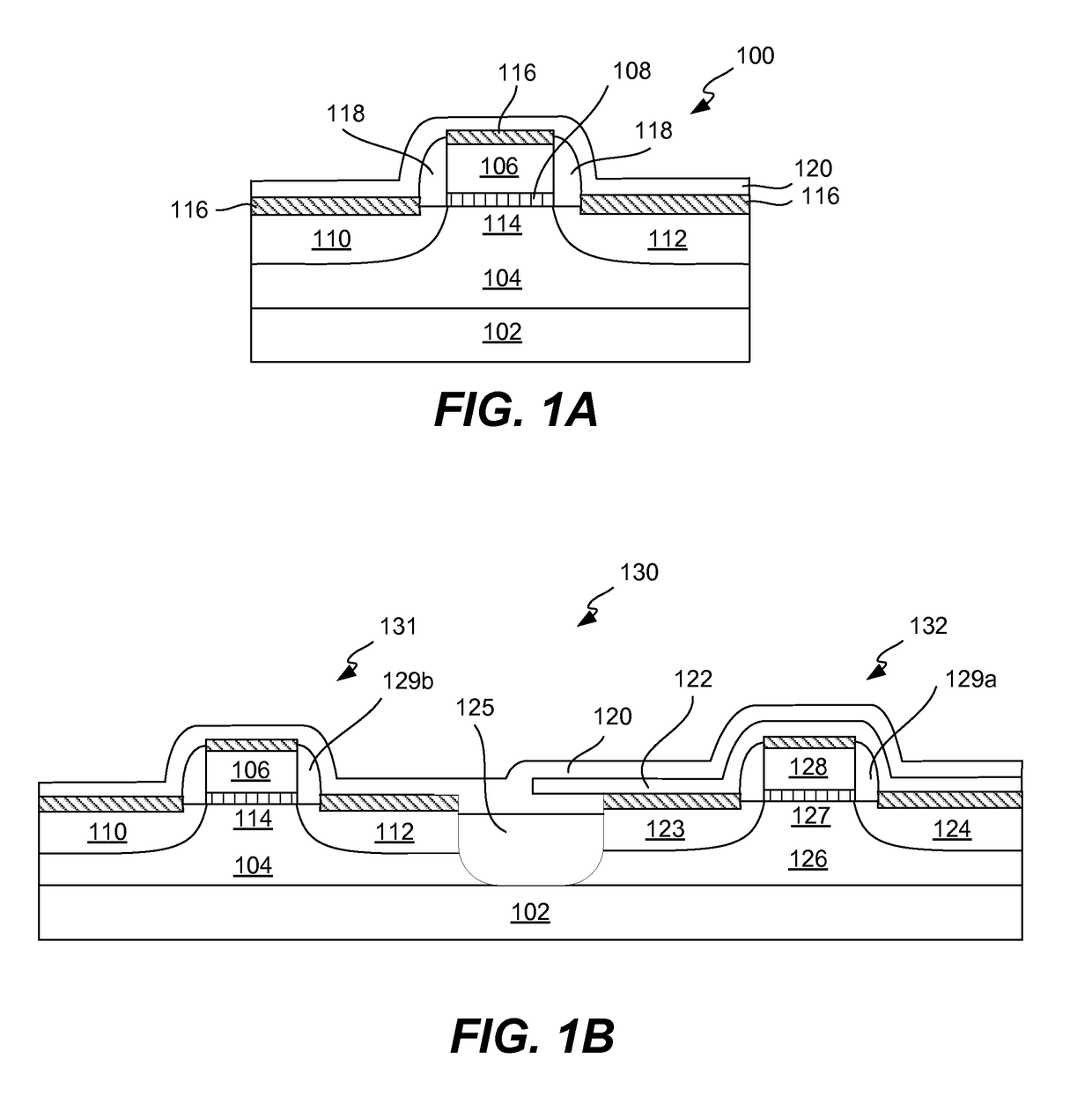
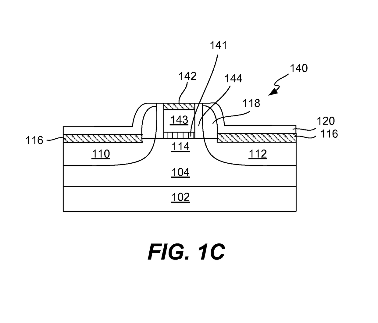
High compressive stress carbon liners for MOS devices
a technology of compressive stress and carbon liners, which is applied in the field of straining transistor architecture of mos devices, can solve the problems of reducing the effective mass of holes, unable to meet the requirements of future transistor generations, and reducing the efficiency of holes, so as to achieve high channel strain without adversely affecting the efficiency of the transistor fabrication process, enhancing the performance of the resulting transistor, and preserving material quality
- Summary
- Abstract
- Description
- Claims
- Application Information
AI Technical Summary
Benefits of technology
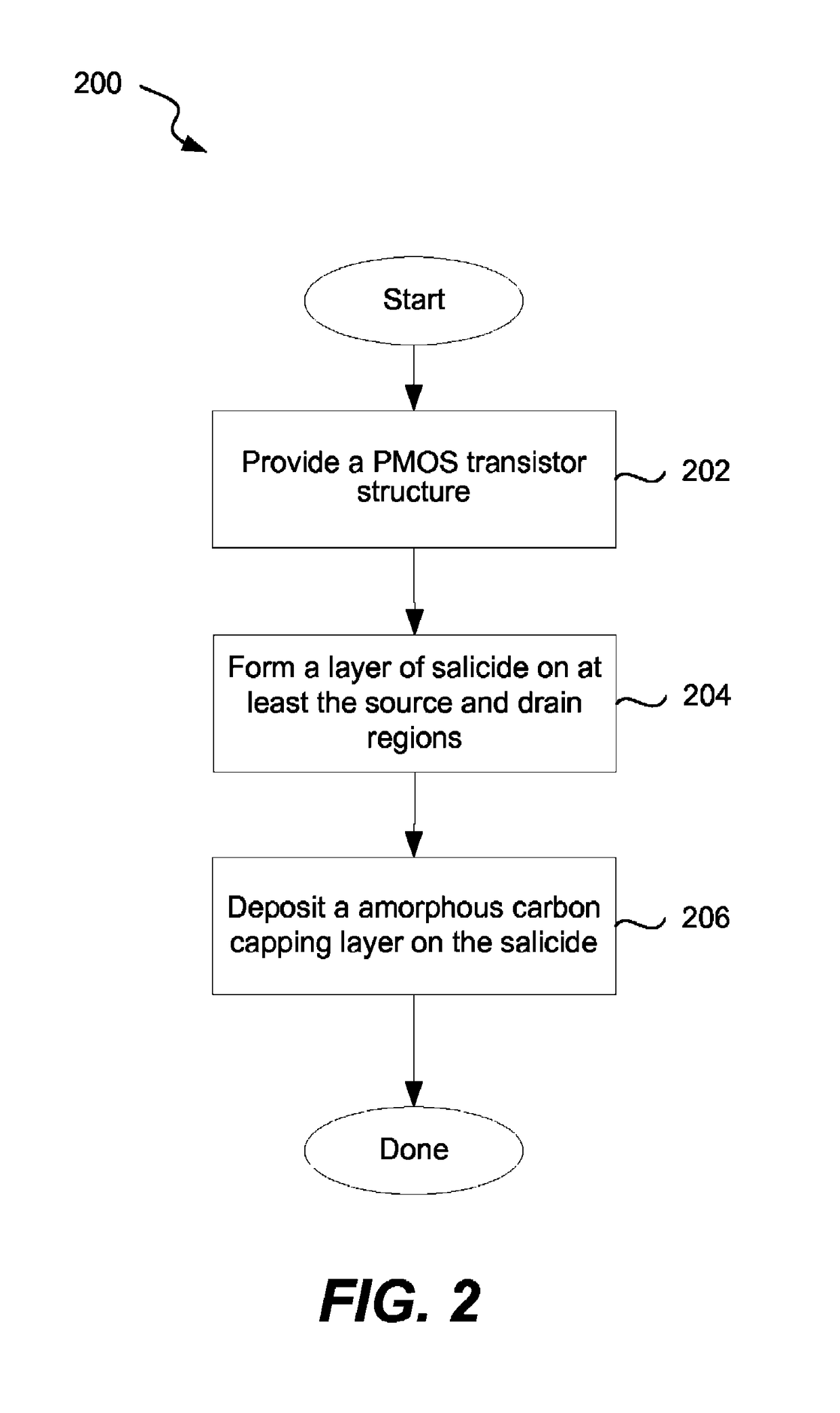
Problems solved by technology
Method used
Image

Examples
example 1
The following example is provided to further illustrate aspects and advantages of the present invention. This example is provided to exemplify and more clearly illustrate aspects of the present invention and is in no way intended to be limiting.
An amorphous carbon capping layer film was deposited on the silicon substrates of a series of commercially-available silicon semiconductor wafers. The capping layer was deposited on each wafer using a PECVD process in all six RF stations of a Novellus Sequel apparatus. The deposition plasma conditions were the same for all wafers, and are summarized here for the Sequel apparatus as a whole.
The flow rates and the power values for each of the six RF stations corresponded to about one-sixth of the values listed below. Methane was used as a precursor with the flow rate of 200 sccm. The pressure in the reaction chamber was 6 Ton, and the temperature was 380° C. The helium flow rate is 8500 sccm; argon flow rate was 4000 sccm. Nitrogen was not used...
example 2
The following example is provided to further illustrate aspects and advantages of the present invention. This example is provided to exemplify and more clearly illustrate aspects of the present invention and is in no way intended to be limiting.
An amorphous carbon capping layer film was deposited on the silicon substrates of a series of commercially-available silicon semiconductor wafers. The capping layer was deposited on each wafer using a PECVD process in all four RF stations of a Novellus Vector apparatus. The deposition plasma conditions were the same for all wafers, and are summarized here for the Vector apparatus as a whole.
The flow rates and the power values for each of the four RF stations corresponded to about one-fourth of the values listed below. Methane was used as a precursor with the flow rate of 300 sccm. The pressure in the reaction chamber was 6 Ton and the temperature was 380° C. The helium flow rate is 21060 sccm; argon flow rate was 14480 sccm. Nitrogen was not ...
PUM
 Abstract
Description
Claims
Application Information