One-transistor, one-resistor, one-capacitor phase change memory

a technology of phase change memory and resistor, which is applied in the field of memory devices, can solve the problems of limited cycle endurance, high reset current, slow set speed, etc., and achieve the effect of fast program/erase speed

Active Publication Date: 2011-04-26
MACRONIX INT CO LTD
View PDF378 Cites 68 Cited by
  • Summary
  • Abstract
  • Description
  • Claims
  • Application Information

AI Technical Summary

Benefits of technology

[0011]A memory cell described herein comprising a transistor, a capacitor and a programmable resistance memory element allows for both volatile and nonvolatile modes of memory operation. The capacitor provides fast program / erase speed, while the programmable resistance memory element provides data retention for nonvolatile data storage. The volatile and nonvolatile modes can provide different operational characteristics such as switching speed, cycle endurance, operational current, and data retention within the same memory cell. As a result, the same memory cell can serve as working memory or nonvolatile memory to address the different memory performance requirements demanded by various functions of an integrated circuit.

Problems solved by technology

However performance limitations such as a relatively slow set speed, a high reset current, and limited cycle endurance has restricted the use of phase change based memory circuits as high speed random access memory for the integrated circuit.
However, integration of different types of memory circuits for the various memory applications in an integrated circuit can be difficult and result in highly complex designs.

Method used


Image

  • One-transistor, one-resistor, one-capacitor phase change memory
  • One-transistor, one-resistor, one-capacitor phase change memory
  • One-transistor, one-resistor, one-capacitor phase change memory

Examples


first embodiment

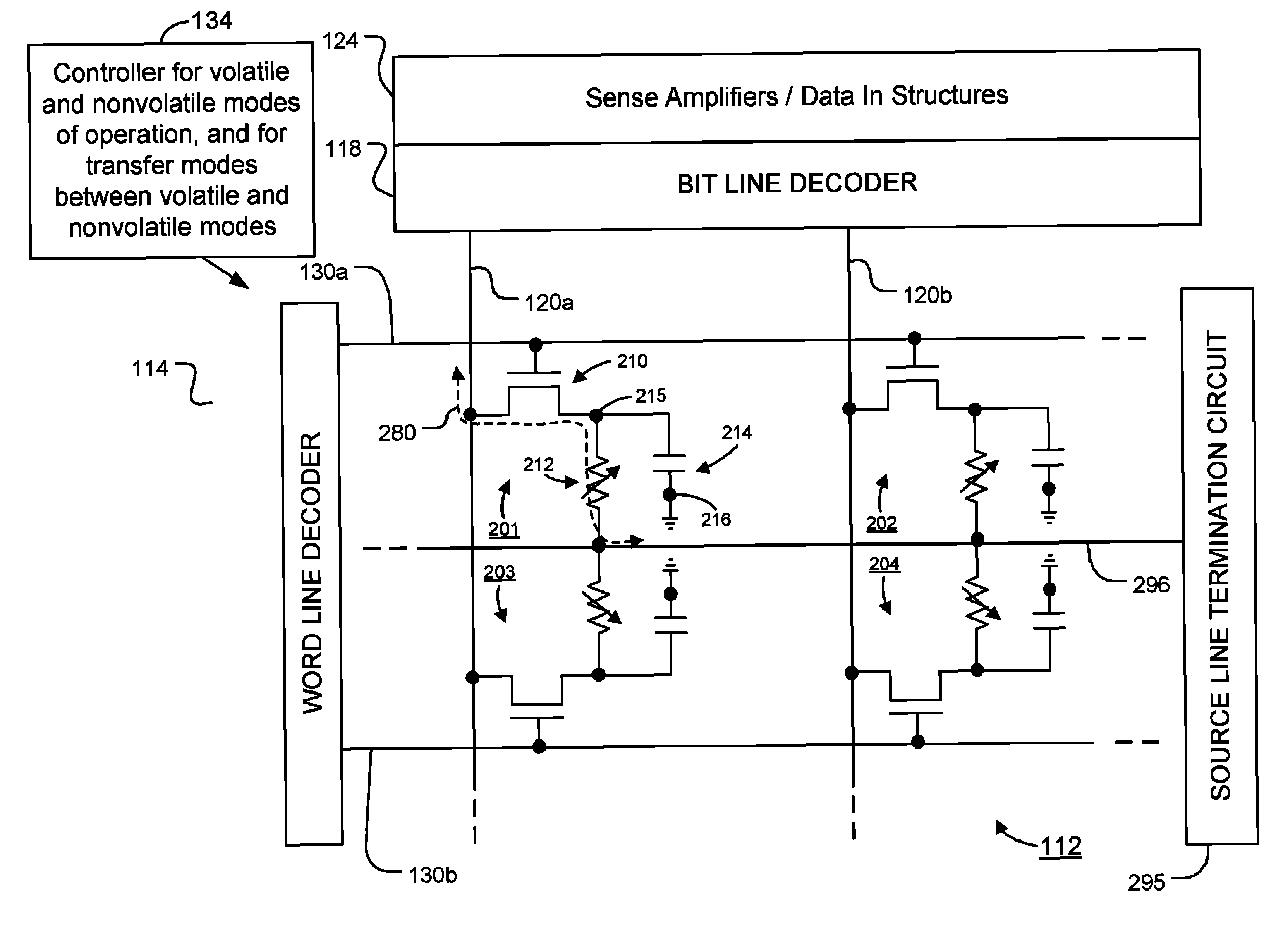
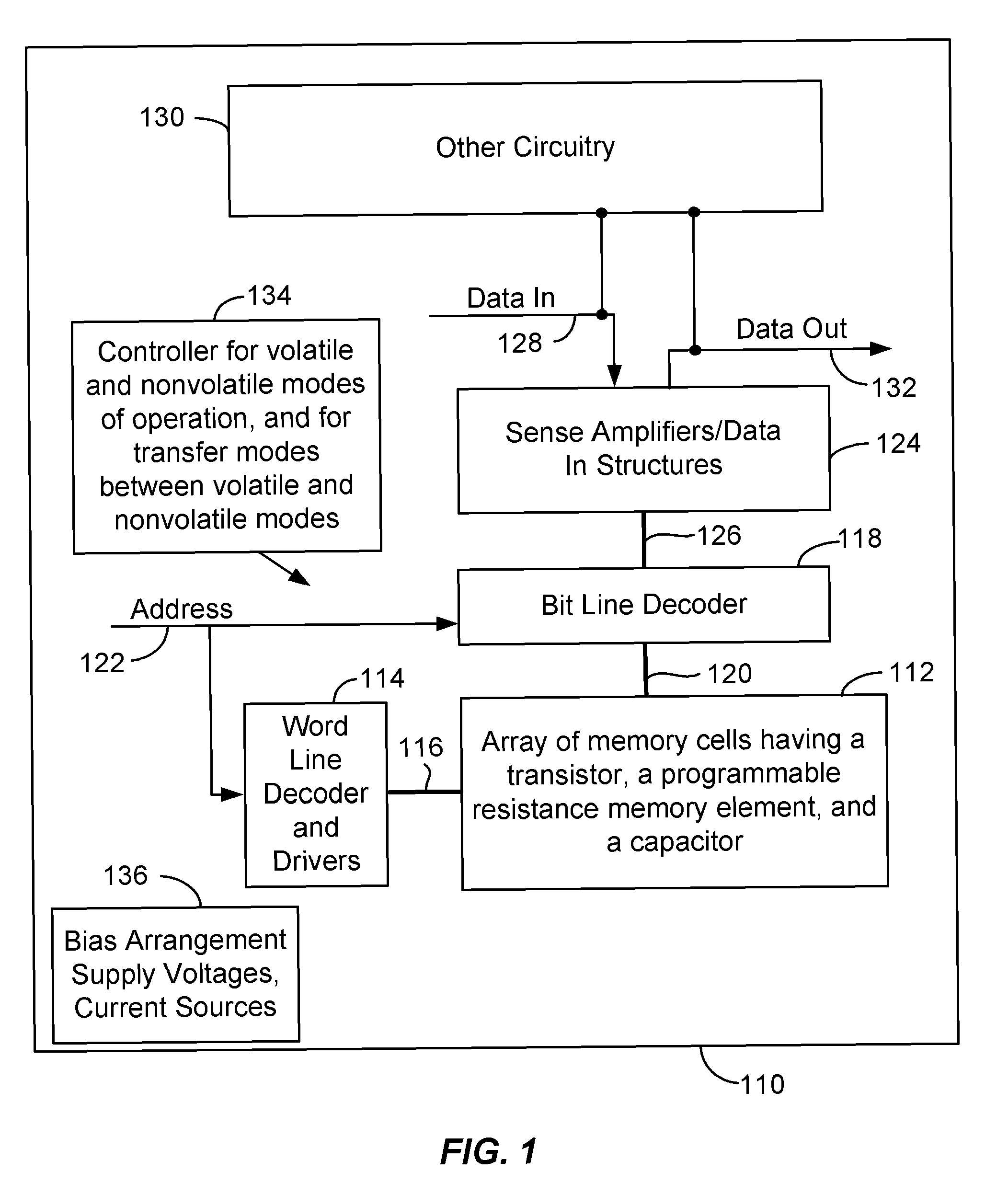
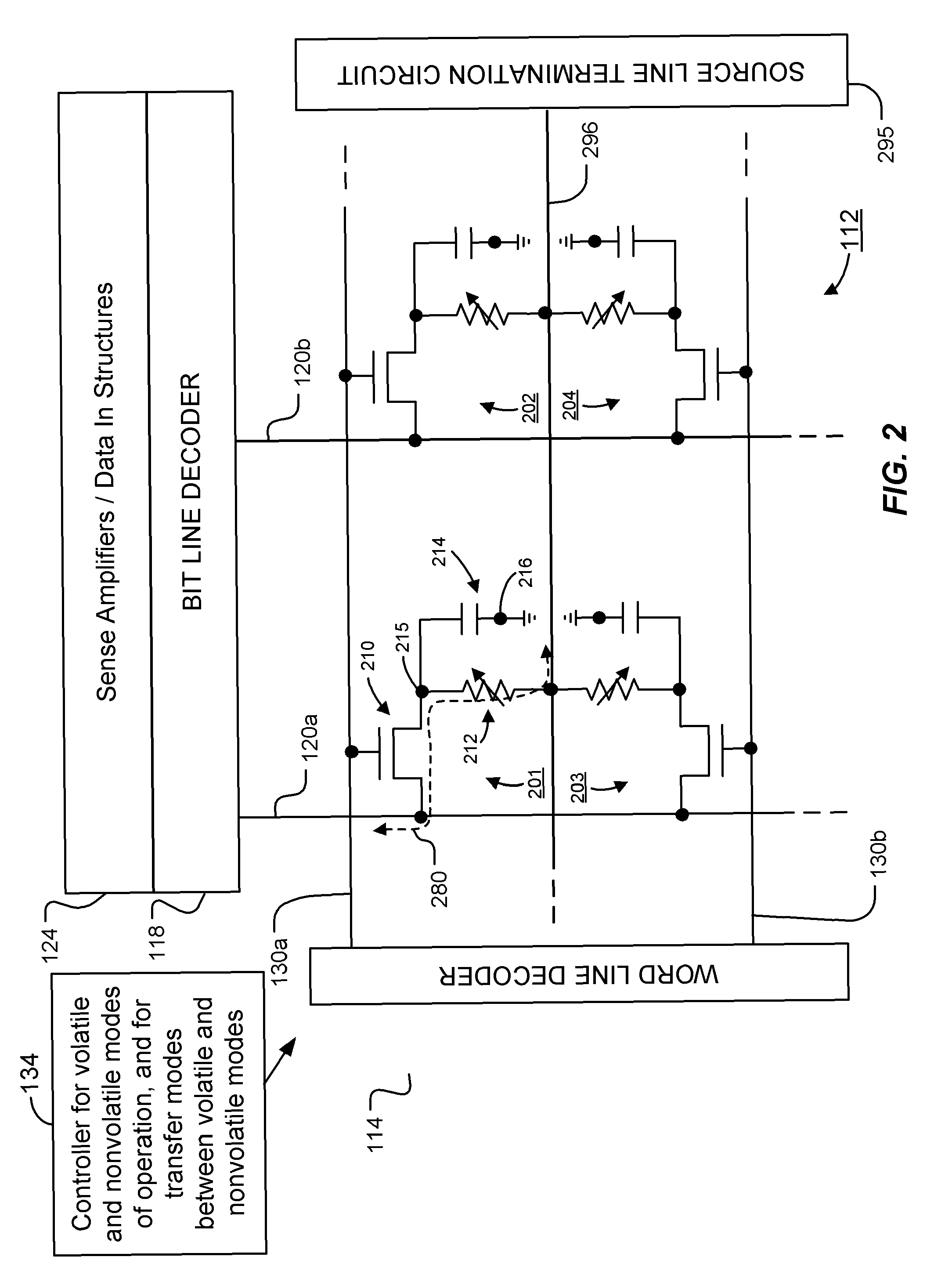
[0034]FIG. 2 illustrates a schematic diagram of array 112 of the integrated circuit 110. Each of the memory cells of the array 112 has a field effect transistor, a programmable resistance memory element (represented as a variable resistor in the Figure), and a charge storage capacitor. Four memory cells 201-204 are illustrated in FIG. 2, representing a small section of the array 112 that can include millions of memory cells. As described in more detail below, each memory cell can be operated as high-speed volatile memory using the capacitor as a data storage element, and can be operated as nonvolatile memory using the programmable resistance memory element as a data storage element. The memory cells can also be operated in a transfer mode to directly transfer a data value stored in the programmable resistance memory element to the capacitor, and vice-versa, without the need for a read operation.

[0035]In FIG. 2 the programmable resistance memory elements couple the sources of the acc...

second embodiment

[0081]FIG. 8 illustrates a schematic diagram of array 112 of FIG. 2. In FIG. 8 the memory cells of the array 112 are implemented using a floating body cell (FBC) which utilizes transient charge storage in the floating channel body of access transistors formed on a silicon on insulator (SOI) or the like. The stored charge causes a detectable shift in the threshold voltage of the access transistor, which is used to indicate stored data. Additional details concerning floating body cells can be seen, for example, in Nitayama et al., “Overview and Future Challenge of Floating Body Cell (FBC) Technology for Embedded Applications”, International Symposium on VLSI Technology, Systems, and Applications, April 2006, pp. 1-3, which is incorporated by reference herein. See also U.S. Pat. No. 7,208,799 and U.S. Pat. No. 6,661,042, both of which are incorporated by reference herein.

[0082]The floating channel body takes the place of a discrete capacitor by using the capacitance formed between the ...


PUM


Abstract

Memory devices and methods for operating such devices are described herein. A memory cell as described herein comprises a transistor electrically coupled to first and second access lines. A programmable resistance memory element is arranged along a current path between the first and second access lines. A capacitor is electrically coupled to the current path between the first and second access lines.

Description

[0001]International Business Machines Corporation, a New York corporation, and Macronix International Corporation, Ltd, a Taiwan corporation, are parties to a Joint Research Agreement.BACKGROUND OF THE INVENTION[0002]1. Field of the Invention[0003]The present invention relates to memory devices based on phase change based memory materials, including chalcogenide based materials and other programmable resistance materials, and methods for operating such devices.[0004]2. Description of Related Art[0005]In general, system-on-a-chip (SOC) technology is the integration of multiple subsystems of electronic system within a single integrated circuit, and may contain digital, analog, mixed-signal, and radio-frequency functions. The various types of subsystems that may be integrated within the integrated circuit include microprocessor and microcontroller cores, digital signal processors (DSPs), configurable logic units, memory blocks, timing sources, external interfaces, and power management ...

Claims


Application Information

Patent Timeline
Patent Type & Authority Patents(United States)
IPC IPC(8): G11C11/00
CPCG11C11/5614G11C11/4076G11C11/5685G11C13/0004G11C13/0007G11C13/0011G11C13/0033G11C13/0069G11C16/3431H01L27/2436H01L45/04H01L45/06H01L45/085H01L45/1233H01L45/142H01L45/144H01L45/146H01L45/1625H01L45/1641G11C11/404G11C11/5678G11C2213/31G11C2213/32G11C2213/79G11C14/0045H10B63/30H10N70/245H10N70/231H10N70/20H10N70/8822H10N70/826H10N70/8828H10N70/8833H10N70/026H10N70/041
Inventor LUNG, HSIANG-LAN
Owner MACRONIX INT CO LTD
Why Eureka
Try Eureka