High speed carbon nanotube memory

a carbon nanotube and memory technology, applied in the field of integrated circuits, can solve the problems of increasing driving current and rc delay time, reducing cell efficiency, and difficult to latch the sense amp output at high speed, and achieve the effect of quick discharge and increased density

Inactive Publication Date: 2011-04-26
KIM JUHAN
View PDF7 Cites 13 Cited by
  • Summary
  • Abstract
  • Description
  • Claims
  • Application Information

AI Technical Summary

Benefits of technology

[0009]For realizing high speed carbon nanotube memory, local bit line is multi-divided into short line for reducing parasitic capacitance, which realizes fast read / write operation with fast charging / discharging time. And, a small local sense amp is realized for reading a data in a memory cell through lightly loaded local bit line, such that the local sense amp is composed of a local write circuit, a local pre amplifier and a local main amplifier, where a source line of the local pre amplifier is connected to a middle voltage VM as a reference voltage for detecting whether the local bit line is higher than that of the VM voltage which is also forced to the local bit line as a pre-charge voltage. In doing so, no waiting time is required for enabling the local pre amplifier after a word line is turned on, because the local pre amplifier discharges a local pre-amp node when reading data “1”, otherwise the local pre amplifier does not discharge the local pre-amp node, when reading data “0”. And a global sense amp is connected to the local sense amp through a read global bit line for reading an output of the local sense amp.
[0011]And, configuring memory is more flexible, such that multiple memory macros can be easily configured with small segmented memory array and multi-stage sense amps, instead of big macro with the conventional sense amps. And number of sense amps can be determined by the target speed. For example, high speed application needs more segmented array with more sense amps, while high density application needs more memory cells with reduced number of sense amps, thus cell efficiency is increased.
[0014]More specifically, a reference signal is generated by one of fast changing data with high gain from reference cells, which signal serves as a reference signal to generate a locking signal for the output latch circuit in order to reject latching another data which is slowly changed with low gain, such that high voltage data is arrived first while low voltage data is arrived later, or low voltage data is arrived first while high voltage data is arrived later depending on configuration. The time-domain sensing scheme effectively differentiates high voltage data and low voltage data with time delay control, while the conventional sensing scheme is current-domain or voltage-domain sensing scheme with a heavy bit line pair. There are many advantages to realize the time-domain sensing scheme, so that the sensing time is easily controlled by a tunable delay circuit, which compensates cell-to-cell variation and wafer-to-wafer variation, such that there is a need for adding a delay time before locking the output latch circuit with a statistical data for all the memory cells, such as mean time between fast data and slow data. Thereby the tunable delay circuit generates a delay for optimum range of locking time. And the read output from the memory cell is transferred to the output latch circuit through a returning read path, thus the access time is equal regardless of the location of the selected memory cell, which is advantageous to transfer the read output to the external pad at a time.
[0015]And, the current flow of the pass transistor of the memory cell can be reduced because the pass transistor only drives a lightly loaded local bit line, which means that the pass transistor can be miniaturized further. Moreover, the present invention realizes multi-stacked memory cell structure including thin film transistor because the memory cell only drives lightly loaded bit line even though thin film polysilicon transistor can flow lower current, for example, around 10 times lower. Thereby, bit line loading is reduced around 10 times lower for compensating the low current drivability of the pass transistor. There are almost no limits to stack multiple memory cells as long as the flatness is enough to accumulate the memory cell.
[0017]And the fabrication method is compatible with the conventional CMOS process for forming the memory cell. In addition, field-effect aligning process is realized for aligning the carbon nanotubes on exact location of the memory cell, when forming the memory cell. And, the memory cell can be formed from thin film polysilicon layer alternatively, because the lightly loaded bit line can be quickly discharged by the memory cell even though the thin film pass transistor can flow relatively low current. In doing so, multi-stacked memory is realized with thin film transistor, which can increase the density within the conventional CMOS process with additional process steps, because the conventional CMOS process is almost reaching to a scaling limit for fabricating transistors on a surface of a wafer. And, a body-tied TFT (Thin Film Transistor) transistor can be alternatively used as the thin film transistor for alleviating self heating problem of short channel TFT. In doing so, multi-stacked memory is realized with short channel TFT transistor.

Problems solved by technology

And the conventional sense amplifier is relatively big, which reduces cell efficiency.
For example, access time from the sense amp near a data output circuit is faster than that of the sense amp far from the data output circuit, so that it is difficult to latch the sense amp output at high speed, because a latching clock is fixed (not shown).
Furthermore, read data line is also heavily loaded for connecting to multiple memory blocks with no buffers, which increases driving current and RC delay time as well.

Method used


Image

  • High speed carbon nanotube memory
  • High speed carbon nanotube memory
  • High speed carbon nanotube memory

Examples


Embodiment Construction

)

[0032]Reference is made in detail to the preferred embodiments of the invention. While the invention is described in conjunction with the preferred embodiments, the invention is not intended to be limited by these preferred embodiments. On the contrary, the invention is intended to cover alternatives, modifications and equivalents, which may be included within the spirit and scope of the invention as defined by the appended claims. Furthermore, in the following detailed description of the invention, numerous specific details are set forth in order to provide a thorough understanding of the invention. However, as is obvious to one ordinarily skilled in the art, the invention may be practiced without these specific details. In other instances, well-known methods, procedures, components, and circuits have not been described in detail so that aspects of the invention will not be obscured.

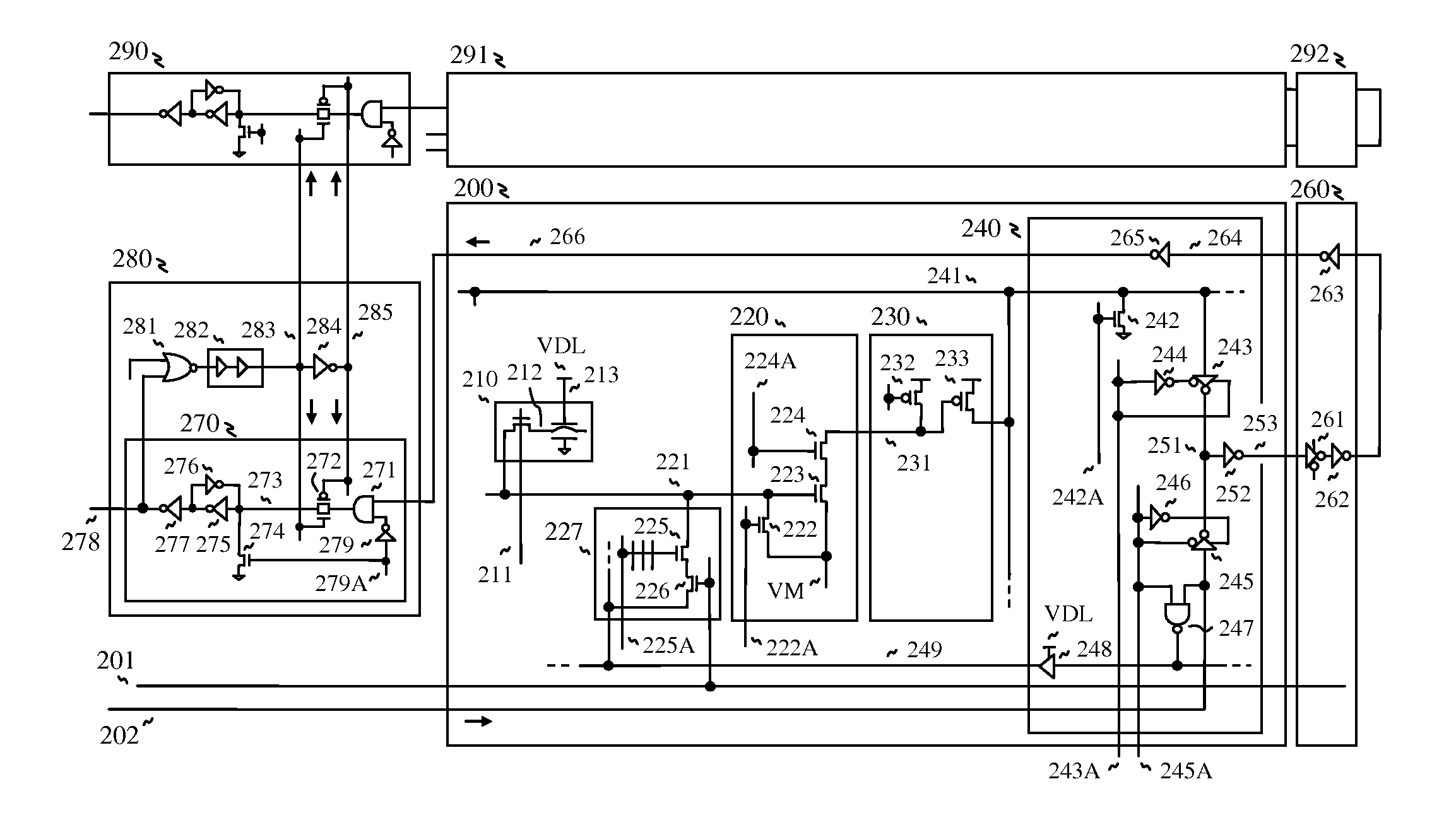
[0033]The present invention is directed to high speed carbon nanotube memory as shown in FIG. 2A, w...


PUM


Abstract

In order to realize high speed carbon nanotube memory, bit line is multi-divided into short lines for reducing parasitic capacitance. For reading, a small local sense amp is composed of a local pre amplifier and a local main amplifier with high gain, and a simple global sense amp is composed of an inverter as amplifying circuit for receiving an output of the local sense amp through a global bit line. By the sense amps, time domain sensing scheme is realized such that a voltage difference in the bit line is converted to a time difference as an output of the global sense amp, for differentiating high data and low data. In this manner, fast read operation is realized with fast sensing circuit. And alternative circuits are described. Particularly, field-effect alignment process is realized for aligning the carbon nanotubes on exact location of the memory cell, when forming the memory cell.

Description

FIELD OF THE INVENTION[0001]The present invention relates generally to integrated circuits, in particular to high speed carbon nanotube memory.BACKGROUND OF THE INVENTION[0002]Carbon nanotube has been demonstrated to have remarkable physical, electrical and thermal properties, and is likely to find numerous applications such as a high-speed and high-density nonvolatile memory. In order to store data, the carbon nanotube is bended to one of two electrodes, which exhibits high voltage or low voltage depending on the bended carbon nanotube.[0003]In FIG. 1A, a prior art of carbon nanotube-based memory circuit including carbon nanotube and sense amplifier is illustrated, as published, U.S. Pat. No. 7,112,493, U.S. Pat. No. 7,115,901 and U.S. Pat. No. 7,113,426. The memory cell 130 is consisted of MOS transfer transistor 132 and carbon nanotube storage element (NT). The transfer gate 132, the drain / source 134 and 135 configure MOS transistor. And storage node (SN), reference node (REF) an...

Claims


Application Information

Patent Timeline
Patent Type & Authority Patents(United States)
IPC IPC(8): G11C7/02
CPCB82Y10/00G11C13/004G11C15/046G11C13/025G11C2213/79G11C2213/16
Inventor KIM, JUHAN
Owner KIM JUHAN
Why Eureka
Try Eureka