Method for fabricating PMOS transistor and method for forming dual gate using the same

a technology of pmos transistor and dual gate, which is applied in the direction of semiconductor devices, electrical equipment, basic electric elements, etc., can solve the problems of ring oscillator delay, low mass productivity, and limitation of pmos transistor with buried channel, and achieve the effect of effectively doping a polysilicon layer

Active Publication Date: 2011-05-03
SK HYNIX INC
View PDF3 Cites 6 Cited by
  • Summary
  • Abstract
  • Description
  • Claims
  • Application Information

AI Technical Summary

Benefits of technology

[0007]Embodiments of the present invention are directed to a method for fabricating a PMOS transistor which can effectively dope a polysilicon layer utilizing existing equipments without purchasing new equipments, and a method of forming a dual gate using the same.

Problems solved by technology

However, as a design rule is decreased more and more and high power and high speed operation are required, the PMOS transistor with the buried channel represents a limitation.
However, the method of doping the polysilicon layer by the ion implantation takes more than 30 minutes per a wafer for implanting a large amount of P-type dopant and has a problem of low mass productivity.
Such oxide layer formed between the polysilicon layer and the tungsten layer causes ring oscillator delay.
Also, in the case of the plasma doping, it is necessary to purchase a new plasma doping equipment of high price.

Method used


Image

  • Method for fabricating PMOS transistor and method for forming dual gate using the same
  • Method for fabricating PMOS transistor and method for forming dual gate using the same
  • Method for fabricating PMOS transistor and method for forming dual gate using the same

Examples


Embodiment Construction

[0015]Hereinafter, an exemplary embodiment of the present invention will be described with reference to accompanying drawings. The embodiment is for illustrative purposes only, and the scope of the present invention is not limited thereto.

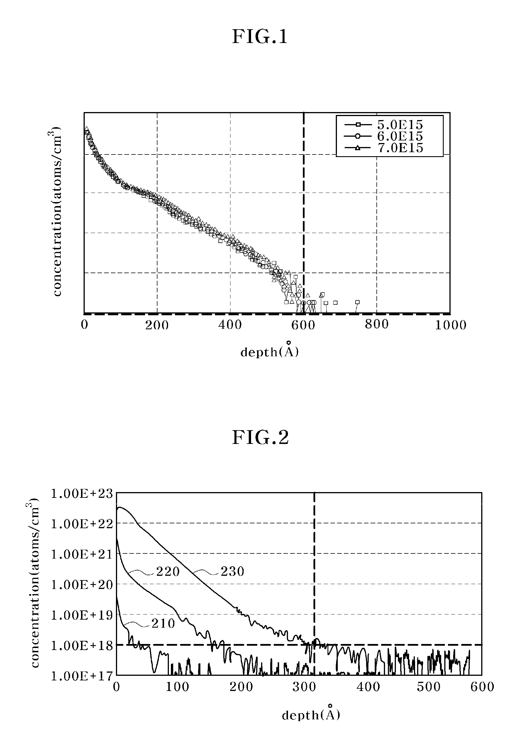
[0016]FIG. 1 is a graph showing a SIMS profile of a polysilicon layer doped with boron (B) ion using a plasma doping and shows a doping profile according to a depth of a polysilicon layer in cases that 11 B ions are implanted at a concentration of 5.0×10¹⁵ions / cm3, 6.0×10¹⁵ions / cm3 and 7.0×10¹⁵ions / cm3, respectively.

[0017]It can be seen that the boron ions have reached to a depth of about 600 Å in all of the three cases using a plasma doping.

[0018]FIG. 2 is a graph showing a SIMS profile of a polysilicon layer doped with boron (B) ion using Atomic Layer Deposition (ALD) and Chemical Vapor Deposition (CVD) equipments.

[0019]A reference numeral “210” indicates a case of doping a bare wafer, “220” indicates a case of soaking for 60 seconds at a tempera...


PUM

PropertyMeasurementUnit
temperatureaaaaaaaaaa

Abstract

Provided are a method for fabricating a PMOS transistor and a method for forming a dual gate of a semiconductor device using the same. The method for fabricating a PMOS transistor includes forming a gate insulation layer over a semiconductor substrate; forming a polysilicon layer over the gate insulation layer; and doping the polysilicon layer using a boron (B) containing gas in one of an Atomic Layer Deposition (ALD) chamber and a Chemical Vapor Deposition (CVD) chamber.

Description

CROSS-REFERENCE TO RELATED APPLICATIONS[0001]The present application claims priority to Korean patent application number 10-2008-0111581, filed on Nov. 11, 2008, which is incorporated by reference in its entirety.BACKGROUND OF THE INVENTION[0002]The present invention relates to a method for fabricating a semiconductor device, and more particularly, to a method for fabricating a PMOS transistor and a method for forming a dual gate of a semiconductor device using the same.[0003]Polysilicon is generally used as a material for forming a gate of a semiconductor device. This is because the polysilicon meets physical properties required for the gate material such as high melting point, easiness of thin film formation and line pattern formation and formability of an even surface. Conventionally, for process simplification, the gate is formed of N-type doped polysilicon in both NMOS and PMOS transistors and the PMOS transistor is therefore formed with a buried channel. However, as a design r...

Claims


Application Information

Patent Timeline
Patent Type & Authority Patents(United States)
IPC IPC(8): H01L21/8238
CPCH01L21/223H01L21/823842H01L21/28035H01L29/78H01L29/4925
Inventor ROUH, KYOUNG BONGKIM, CHOON HWANRHO, IL CHEOL
Owner SK HYNIX INC
Why Eureka
Try Eureka