Method of preparing group III-V compound semiconductor crystal

a technology of compound semiconductor crystals and semiconductor crystals, which is applied in the direction of polycrystalline material growth, under a protective fluid, gel state, etc., can solve the problems of difficult control of carbon concentration, inability to adjust carbon concentration, and impurity contamination, so as to achieve greater effect, increase purity, and prolong heat treatment time

Inactive Publication Date: 2007-08-21
SUMITOMO ELECTRIC IND LTD
View PDF34 Cites 2 Cited by
  • Summary
  • Abstract
  • Description
  • Claims
  • Application Information

AI Technical Summary

Benefits of technology

[0024]In the present invention, the amount of solid carbon to be filled into the crucible is preferably larger than the amount of carbon to be doped into the compound semiconductor crystal. This is to promote reaction using an excessive amount of carbon since the reaction rate of solid carbon is extremely low. Furthermore, an additional amount of carbon must be supplied to make up for the consumption of part of the solid carbon in gas generation of the carbon compound. Thus, by using solid carbon of an amount larger than the total amount of carbon doped into the crystal, the advantage of the present invention works effectively. Specifically, the amount of solid carbon must be at least ten times, preferably at least 100 times larger than the weight of the carbon doped into the crystal.
[0025]In the present invention, it is preferred that the solid carbon is subjected to a heat treatment under reduced pressure before being filled in the crucible or boat. By this process, any impurity element remaining in the carbon is removed to result in a crystal of higher purity. The pressure in applying the heat treatment to the carbon is preferably from 1 Torr to 1×10⁻⁸ Torr. The appropriate temperature of the heat treatment is 500° C.-2000° C. The above-described effect can be obtained by carrying out the heat treatment for at least one hour. It was found that a greater effect can be obtained as the time for the heat treatment becomes longer. However, there is very little further change in the effect when the time for the heat treatment exceeds 12 hours. Considering that the cost for production is increased as the time for the heat treatment becomes longer, the time period for the heat treatment of not more than 12 hours is appropriate.
[0026]In the present invention, it is preferable to keep the compound raw material in its melted state for a certain time period before it is solidified for crystal growth. By this process, the impurities of Si and the like in the GaAs polycrystalline raw material can be removed by gettering with boron oxide. Although Si of approximately 1×1016cm−3 is included as impurities in the raw material synthesized by the HB method, the amount of Si in the GaAs subjected to the above-described process is less than 1×1015cm−3, which is below the detection limit of an analyzer. Si of an amount over 1×1015cm−3 was detected from those samples not subjected to the above-described process.
[0027]Thus, carbon can be sufficiently melted in the GaAs melt from the solid carbon by the above-described process. This process also provides the advantage that the temperature of the GaAs melt is stabilized, and the carbon concentration and impurity concentration in the melt can be made uniform.
[0028]The above-described effect can be obtained when the holding time period in the melted state of raw material is at least 3 hours. Further favorable characteristics can be obtained stably when the holding time is at least 6 hours. Although a greater effect can be obtained as the holding time becomes longer, the degree of change in the effect gradually becomes smaller when the holding time period exceeds 36 hours. There is very little further change in the effect when the holding time exceeds 72 hours. Considering that the cost for production becomes higher as the holding time is increased, the holding time is preferably not more than 72 hours, further preferably not more than 36 hours.
[0029]In the present invention, powder carbon can be used as the solid carbon. Powder carbon is advantageous in promoting the reaction due to its greater specific surface area. Increase in the reaction speed allows carbon to be doped efficiently in the crystal.

Problems solved by technology

Therefore, impurity contamination can be expected.
Furthermore, since the amount of the carbon source cannot be controlled in this method, it is difficult to control the carbon concentration.
There is a problem that the carbon concentration cannot be adjusted during crystal preparation.
Furthermore, a part of the carbon in the GaAs melt reacts with oxygen, which is generated as a result of the water in the boron oxide decomposing, to be lost as CO gas.
As a result, there is a problem that the carbon concentration in the GaAs crystal is lowered.
In prior art 3, it is difficult to control the carbon concentration since the carbon source is located outside the crucible.
Furthermore, impurity contamination can be expected since boron oxide is not used.

Method used


Image

  • Method of preparing group III-V compound semiconductor crystal
  • Method of preparing group III-V compound semiconductor crystal
  • Method of preparing group III-V compound semiconductor crystal

Examples


example 1

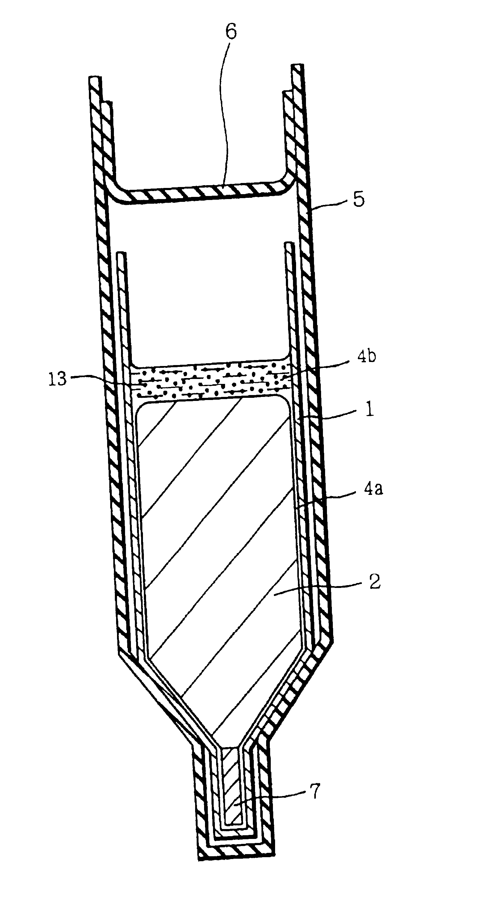
[0045]FIG. 1 is a diagram for describing an example of preparing a group III-V compound semiconductor crystal according to the present invention. Referring to FIG. 1, GaAs polycrystalline raw material 2, carbon powder 13 which has been subjected to heat treatment under reduced pressure in advance, boron oxide (B2O3) 4 forming a boron oxide layer 4b and a boron oxide film 4a as described below, and a seed crystal 7 were placed in a pBN crucible 1. The seed crystal 7 was placed at the bottom portion of the crucible 1. In crucible 1, the materials were so arranged that carbon powder 13 and boron oxide 4 were brought into contact with each other, and also boron oxide 4 and raw material 2 were brought into contact with each other when the raw material was melted.

[0046]Crucible 1 was inserted in a quartz ampoule 5 together with solid arsenic. Ampoule 5 was sealed under reduced pressure with a quartz cap 6.

[0047]Respective conditions of Example 1 are shown in the following Table 1.

[0048]

TA...

example 2

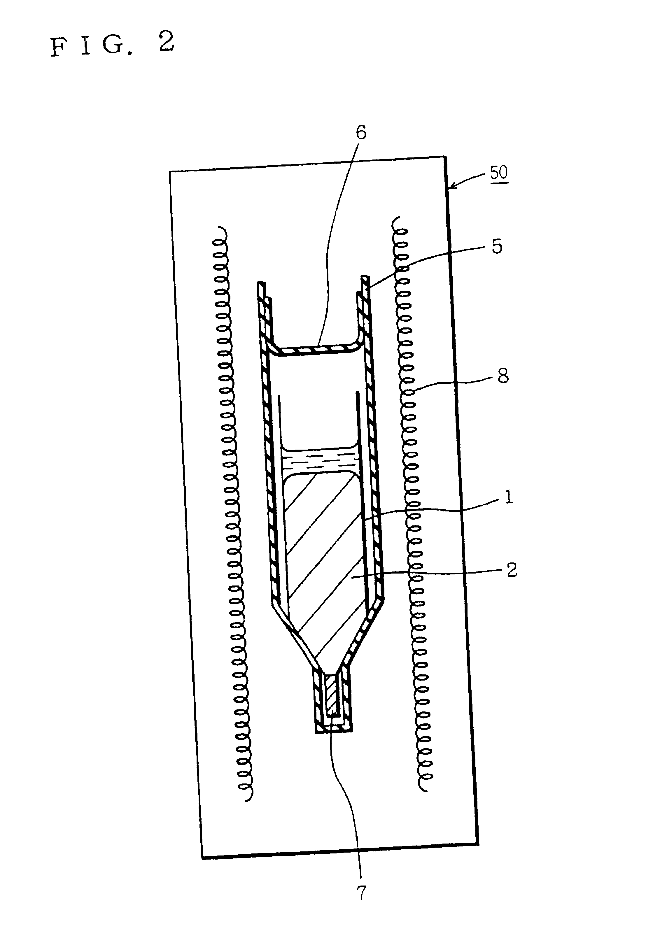
[0054]FIG. 3 is a diagram for describing another example of a method of preparing a group III-V compound semiconductor crystal of the present invention. Referring to FIG. 3, GaAs polycrystalline raw material 2, carbon fiber 23 subjected to heat treatment under reduced pressure in advance, boron oxide 4 forming a boron oxide layer 4b and a boron oxide film 4a as described below, and a seed crystal 7 were placed in a pBN crucible 1. Seed crystal 7 was placed at the bottom portion of the crucible 1. In crucible 1, the materials were arranged so that carbon fiber 23 and boron oxide 4 were brought into contact with each other and also boron oxide 4 and raw material 2 were brought into contact with each other when the raw material was melted. Crucible 1 was inserted into a quartz ampoule 5 together with solid arsenic. Quartz ampoule 5 was sealed under reduced pressure with a quartz cap 6. Respective conditions of Example 2 are shown in the following Table 3.

[0055]

TABLE 3GaAs10 kg usedpoly...

example 3

[0059]A carbon-doped GaAs single crystal was grown using 20 mg of carbon fiber similar to that of Example 2. The other conditions of the experiment were identical to those of Example 2, and their description will not be repeated. The characteristics of the obtained single crystal are shown in the following Table 5.

[0060]

TABLE 5Crystal diameter105 mmLength of φ105 mm portion200 mmCarbon concentrationShoulder2.3 × 1015 cm−3Tail2.2 × 1015 cm−3ResistivityShoulder8.8 × 107 ΩcmTail8.4 × 107 ΩcmDislocation densityShoulder1000 cm−2Tail1800 cm−2


PUM

PropertyMeasurementUnit
temperatureaaaaaaaaaa
grain sizeaaaaaaaaaa
diameteraaaaaaaaaa

Abstract

A method is provided for preparing, with high reproducibility, a carbon-doped group III-V compound semiconductor crystal having favorable electrical characteristics and having impurities removed therefrom, and in which the amount of doped carbon can be adjusted easily during crystal growth. This method includes the steps of: filling a crucible with compound raw material, solid carbon, and boron oxide; sealing the filled crucible within an airtight vessel formed of a gas impermeable material; heating and melting the compound raw material under the sealed state in the airtight vessel; and solidifying the melted compound raw material to grow a carbon-doped compound semiconductor crystal.

Description

BACKGROUND OF THE INVENTION[0001]1. Field of the Invention[0002]The present invention relates to a method of preparing a group III-V compound semiconductor crystal, and particularly a carbon-doped group III-V compound semiconductor crystal.[0003]2. Description of the Background Art[0004]Conventionally, there are various prior art methods for preparing a carbon-doped group III-V compound semiconductor crystal, as set forth in the following described publications.[0005]Japanese Patent Laying-Open No. 64-79087 (referred to as “prior art 1” hereinafter) discloses a method of preparing a carbon-doped GaAs single crystal according to the gradient freeze method for horizontal Bridgman method (HB method). FIG. 6 is a diagram for describing a method of preparing a carbon-doped GaAs single crystal according to prior art 1. Referring to FIG. 6, a graphite boat 51 as a carbon source is arranged at one side in a quartz ampoule 55. Raw material which is gallium (Ga) 52 is provided in graphite boa...

Claims


Application Information

Patent Timeline
Patent Type & Authority Patents(United States)
IPC IPC(8): C30B11/04C30B11/00C30B29/40C30B29/42
CPCC30B11/10C30B27/00C30B29/40C30B29/42
Inventor KAWASE, TOMOHIROTATSUMI, MASAMI
Owner SUMITOMO ELECTRIC IND LTD
Why Eureka
Try Eureka