Organic electroluminescent device and display unit
a technology of electroluminescent devices and display units, which is applied in the direction of organic semiconductor devices, thermoelectric devices, organic chemistry, etc., can solve the problems of undesirable color mixing, adversely affecting the light-emitting function, adversely affecting the function of light-emitting layers, etc., and achieves high color purity, long life, and high brightness
- Summary
- Abstract
- Description
- Claims
- Application Information
AI Technical Summary
Benefits of technology
Problems solved by technology
Method used
Image
Examples
examples
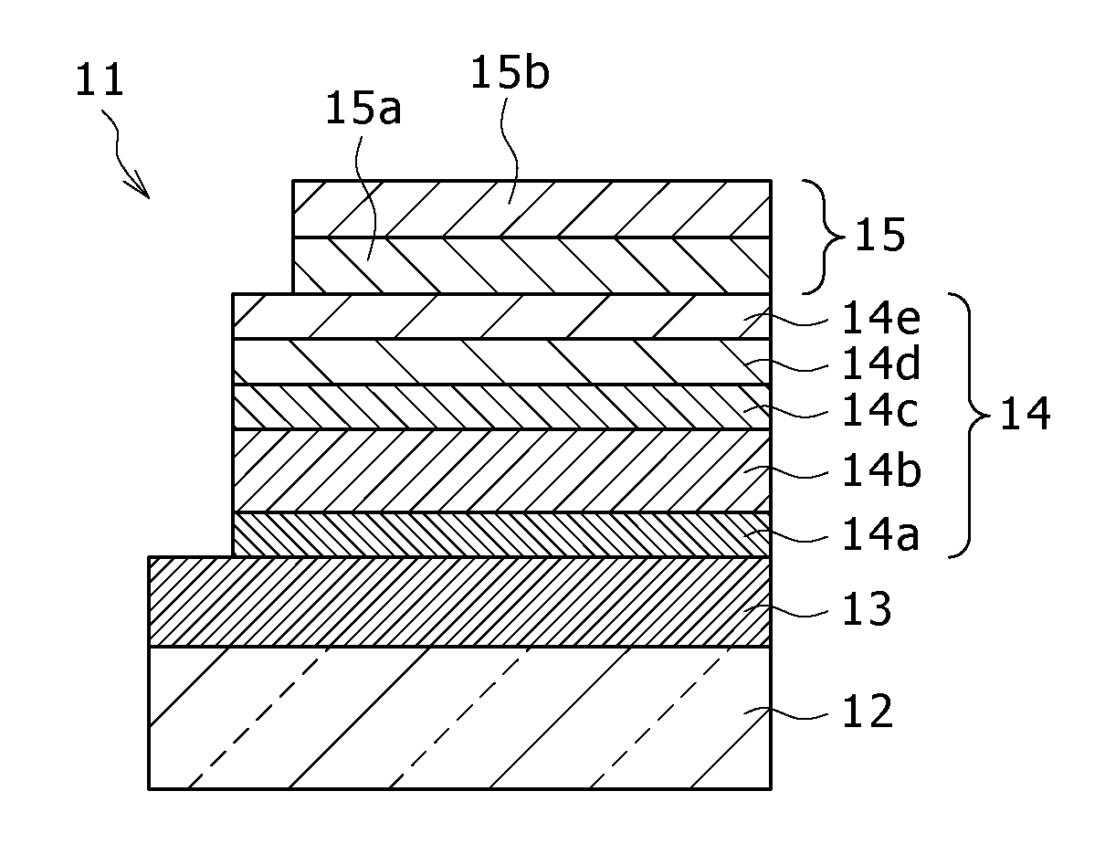
[0111]To illustrate the procedure for production of the organic electroluminescent device according to an embodiment of the present invention, Examples and Comparative Examples are described below with reference to FIG. 1. They are concluded with the result of evaluation of the devices.
examples 1 to 4
[0112]The organic electroluminescent device 11 was produced in the following manner which has the light-emitting layer 14c containing a guest material for blue light emission.
[0113]First, the substrate 12, which is a glass plate measuring 30×30 mm, was coated with a thin film of Ag alloy (190 nm thick) functioning as a reflection layer and a thin film of ITO (12.5 nm thick) functioning as a transparent electrode. These two films constitute the anode 13. The substrate 12 with the anode 13 thereon serves as the cell for the organic electroluminescent device of top emission type.
[0114]On the anode 13 was formed the hole injection layer 14a (12 nm thick) as one constituent of the organic layer 14 by vacuum deposition at a rate of 0.2 to 0.4 nm / sec from m-MTDATA represented by the formula (101) below. m-MTDATA stands for 4,4′,4″-tris(phenyl-m-tolylamino)triphenylamine.
[0115]
[0116]Next, on the hole injection layer 14a was formed the hole transport layer 14b (120 nm thick) by vacuum deposi...
examples 5 and 6
[0132]The organic electroluminescent device 11 was prepared in which the guest material in the light-emitting layer is a green light emitting compound.
[0133]First, the substrate 12, which is a glass plate measuring 30×30 mm, was coated with a thin film of Ag alloy (190 nm thick) functioning as a reflection layer and a thin film of ITO (12.5 nm thick) functioning as a transparent electrode. These two films constitute the anode 13. The substrate 12 with the anode 13 thereon serves as the cell for the organic electroluminescent device of top emission type.
[0134]On the anode 13 was formed the hole injection layer 14a (8 nm thick) as one constituent of the organic layer 14 by vacuum deposition at a rate of 0.2 to 0.4 nm / sec from m-MTDATA represented by the formula (101) above.
[0135]Next, on the hole injection layer 14a was formed the hole transport layer 14b (20 nm thick) by vacuum deposition at a rate of 0.2 to 0.4 nm / sec from A-NPD represented by the formula (102) above.
[0136]On the ho...
PUM
 Abstract
Description
Claims
Application Information


