Capacitor built-in substrate and method of manufacturing the same and electronic component device

a technology of built-in substrates and capacitors, which is applied in the direction of variable capacitors, fixed capacitor details, printed circuit non-printed electric components association, etc., can solve the problems of difficult wiring routes, circuit design restrictions, and insufficient effect of decoupling capacitors, so as to achieve easy manufacturing and large design margin

Inactive Publication Date: 2011-05-03
SHINKO ELECTRIC IND CO LTD
View PDF78 Cites 18 Cited by
  • Summary
  • Abstract
  • Description
  • Claims
  • Application Information

AI Technical Summary

Benefits of technology

[0014]It is an object of the present invention to provide a capacitor built-in substrate in which a capacitor can be arranged in a closer position to a semiconductor chip and be connected thereto and whose margin of design is large, and an electronic component device utilizing the same.
[0020]In the capacitor built-in substrate of the present invention, the connection portions of the first electrodes of the capacitors provided to pass through the base resin layer can be connected directly to the semiconductor chip. Therefore, unlike the prior art, there is no need to route around the wiring connected to the capacitor in the wiring substrate upon connecting the wiring to the semiconductor chip. As a result, the inductance between the semiconductor chip and the capacitors can be reduced, and thus the capacitor built-in substrate can perform enough performances as the decoupling capacitor for the semiconductor chip that operates at a high speed. Also, the through electrode utilized as the signal lines, etc. can be arranged in any position. Therefore, there is no need to arrange the bumps particularly between the semiconductor chip and the wiring substrate, and also a margin of design of the electronic component device can be widened.
[0021]In addition, the metal posts whose height is high are provided to the base resin layer formed of as the high-supple elastic body (polyimide, or the like) and are utilized as the connection bumps. Therefore, the base resin layer and the metal posts function as a stress relaxing layer upon flip-chip connecting the semiconductor chip. As a result, reliability of the electronic component device can be improved.
[0025]The capacitor built-in substrate of the present invention can be easily manufactured by using the above manufacturing method. Also, when the through electrode is built in, the plating opening portions may be formed in portions of the base resin layer on another metal posts after the capacitor is formed, and then the metal bumps may be formed. In addition, the resistor portion can be built in by the same method.

Problems solved by technology

In some cases, an effect of the decoupling capacitor cannot be sufficiently achieved.
Also, in the prior art, such problems have arisen that it is difficult to change the wiring routes because positions of the connection terminals of the capacitor component are restricted, and a circuit design is restricted and a margin of design is small because the die attaching tape must be used, and others.
As a result, the similar problems have arisen.

Method used


Image

  • Capacitor built-in substrate and method of manufacturing the same and electronic component device
  • Capacitor built-in substrate and method of manufacturing the same and electronic component device
  • Capacitor built-in substrate and method of manufacturing the same and electronic component device

Examples


first embodiment

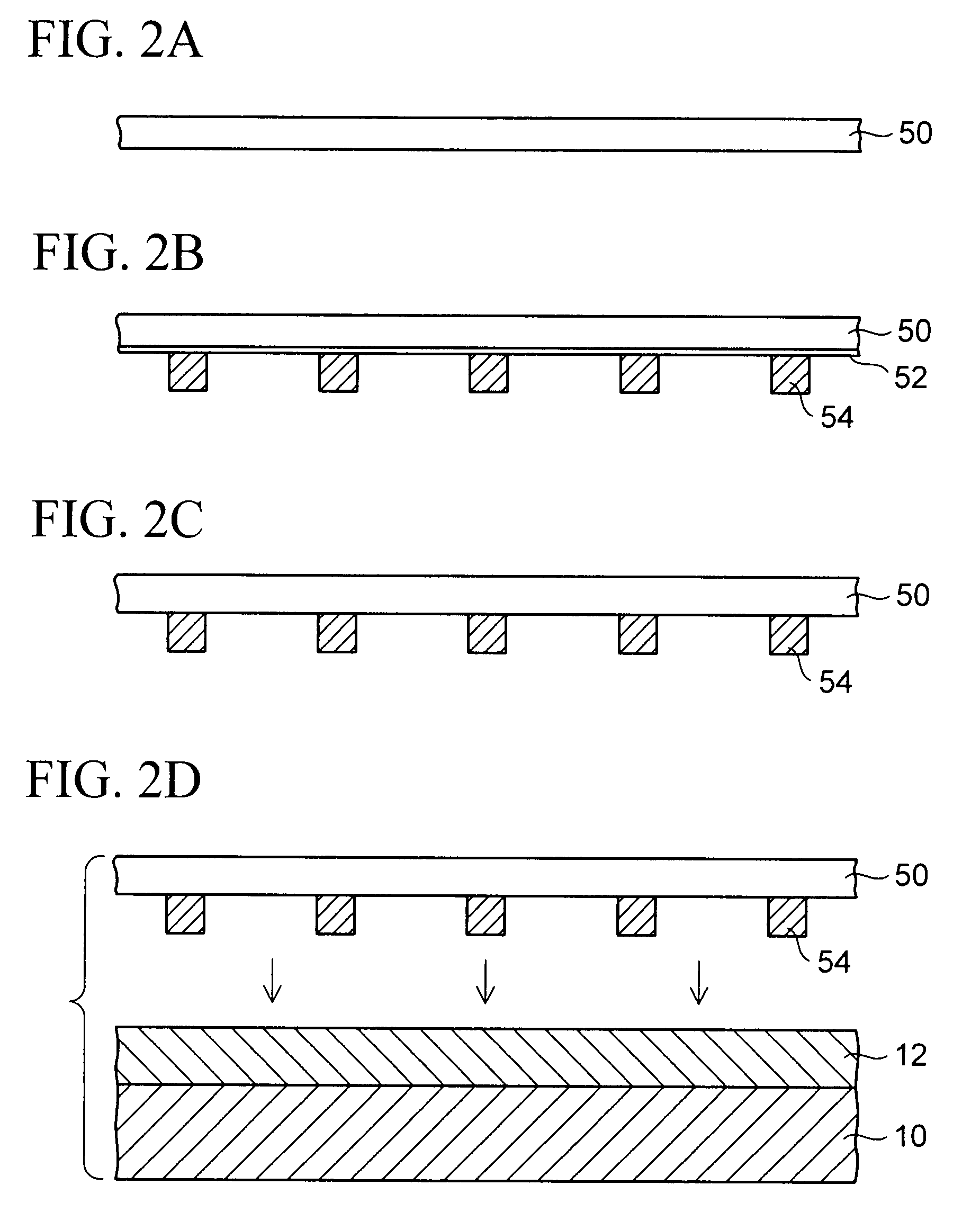
[0036]FIGS. 2A to 2S are sectional views showing a method of manufacturing a capacitor built-in substrate according to a first embodiment of the present invention, and FIG. 3 is a sectional view showing the capacitor built-in substrate similarly.

[0037]In the method of manufacturing the capacitor built-in substrate according to the first embodiment, as shown in FIG. 2A, first, a base resin layer 50 made of a high-supple elastic body such as a polyimide film, an aramid film, or the like and having a film thickness of about 50 μm is prepared. This base resin layer 50 acts finally as an elastic substrate to support a plurality capacitors, and the like. Then, as shown in FIG. 2B, a seed layer 52 made of a copper, or the like is formed on the base resin layer 50 (under the base resin layer 50 in FIG. 2B) by the sputtering.

[0038]Then, a resist film (not shown) in which opening portions are opened in positions where copper posts are formed is formed, and a copper layer is formed in the open...

second embodiment

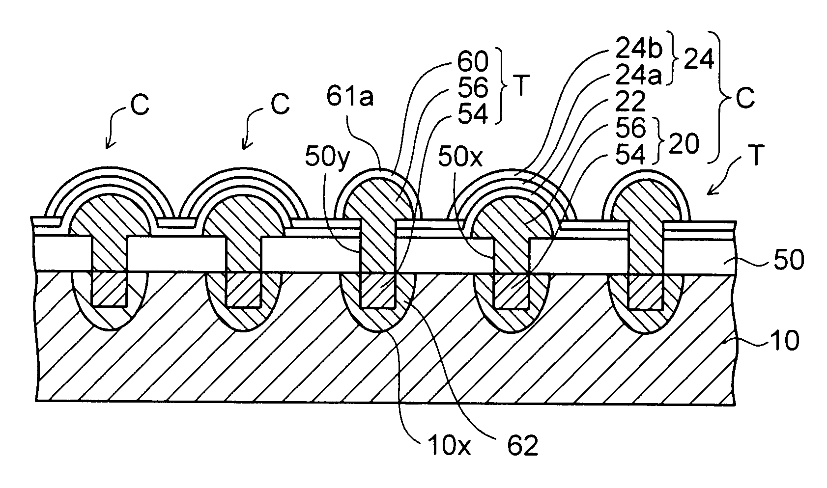
[0075]FIG. 5 is a sectional view showing a capacitor built-in substrate according to a second embodiment of the present invention, and FIG. 6 is a sectional view showing an electronic component device constructed by mounting a semiconductor chip on the capacitor built-in substrate. As shown in FIG. 5, in the capacitor built-in substrate 2 of the second embodiment, resistor portions R in addition to the capacitors C and the through electrodes T are built. In an example in FIG. 5, the through electrode T on the rightmost side in FIG. 3 of the first embodiment constitutes the resistor portion R.

[0076]The resistor portion R is composed of the first electrode 20 made of the copper post 54 and the first copper bump 56 like the first electrode 20 of the capacitor C, an insulating layer 64 formed on the convex curved surface of the first electrode 20 and made of alumina, silicon nitride, titanium nitride, or the like, and a second electrode 66 formed on the insulating layer 64 and made of g...

third embodiment

[0082]FIGS. 7A to 7H are sectional views showing a method of manufacturing a capacitor built-in substrate according to a third embodiment of the present invention. FIG. 8 is a sectional view showing the capacitor built-in substrate similarly. A feature of the third embodiment resides in that the solder layer is utilized finally as the coating layer for the copper post on the basis of filling the solder layer in concave portions provided in the copper plate and then embedding the copper posts in the solder layers. In the third embodiment, detailed explanation of the same steps as those in the first embodiment will be omitted herein.

[0083]In the manufacturing method of the third embodiment, as shown in FIGS. 7A and 7B, the copper plate 10 as a metal supporting body is prepared, and a resist 11 having opening portions 11x is formed on the copper plate 10. Then, concave portions 10x are formed on the copper plate 10 by wet-etching the copper plate 10 through the opening portions 11x in ...


PUM

PropertyMeasurementUnit
thicknessaaaaaaaaaa
heightaaaaaaaaaa
heightaaaaaaaaaa

Abstract

A capacitor built-in substrate of the present invention includes; a base resin layer; a plurality of capacitors arranged side by side in a lateral direction in a state that the capacitors are passed through the base resin layer, each of the capacitors constructed by a first electrode provided to pass through the base resin layer and having projection portions projected from both surface sides of the base resin layer respectively such that the projection portion on one surface side of the base resin layer serves as a connection portion, a dielectric layer for covering the projection portion of the first electrode on other surface side of the base resin layer, and a second electrode for covering the dielectric layer; a through electrode provided to pass through the base resin layer and having projection portions projected from both surface sides of the base resin layer respectively; and a built-up wiring formed on the other surface side of the base resin layer and connected to the second electrodes of the capacitors and one end side of the through electrode.

Description

CROSS-REFERENCE TO RELATED APPLICATIONS[0001]This application is based on and claims priority of Japanese Patent Application No. 2006-217955 filed on Aug. 10, 2006, the entire contents of which are incorporated herein by reference.BACKGROUND OF THE INVENTION[0002]1. Field of the Invention[0003]The present invention relates to a capacitor built-in substrate and a method of manufacturing the same and an electronic component device and, more particularly, a capacitor built-in substrate applicable to a wiring substrate on which a semiconductor chip is mounted and in which a capacitor acting as a decoupling capacitor is built and a method of manufacturing the same and an electronic component device utilizing the same.[0004]2. Description of the Related Art[0005]In the prior art, there is the electronic component device constructed by mounting the semiconductor chip on the wiring substrate in which the decoupling capacitor is built. As shown in FIG. 1, in an example of such electronic com...

Claims


Application Information

Patent Timeline
Patent Type & Authority Patents(United States)
IPC IPC(8): H05K1/16
CPCH01G4/236H01G4/38H01L21/486H01L23/49822H01L23/49827H01L23/50H01L23/642H05K1/162H01G4/33Y10T29/435H01L2221/68345H01L2224/16H01L2924/01078H01L2924/01079H01L2924/04941H01L2924/15311H05K1/113H05K3/007H05K3/20H05K3/4007H05K3/4644H05K2201/0179H05K2201/09763H05K2203/0152H05K2203/0733H01L2224/16265
Inventor MASHINO, NAOHIRO
Owner SHINKO ELECTRIC IND CO LTD
Why Eureka
Try Eureka