Molecular wire crossbar logic (MWCL)

a crossbar logic and molecular wire technology, applied in the field of electronic devices, can solve the problems of direct writing a wafer full of complex devices, each containing trillions of components, and the limit of the miniaturization that has accompanied the growth of si ics, and achieve the effect of reducing the cost of implementation, and reducing the complexity of the control layer

Inactive Publication Date: 2011-05-24
HEWLETT-PACKARD ENTERPRISE DEV LP +2
View PDF1 Cites 5 Cited by
  • Summary
  • Abstract
  • Description
  • Claims
  • Application Information

AI Technical Summary

Benefits of technology

[0014]A major advantage of the present invention is that the logic array is self-assembling. It is an extremely regular structure, which can be assembled using chemical reactions. This is in contrast to lookup tables (LUTs). Although the memory of a LUT is very regular, it requires a decode / demultiplex structure for each instance of the LUT. A demultiplexer is rather irregular and difficult to make chemically, and a very large number of the demultiplexers are needed, about one demultiplexer for every ten logic gates. In contrast to the use of only LUTs, the molecular wire crossbar logic can be assembled chemically.

Problems solved by technology

However, because of a combination of physical and economic reasons, the miniaturization that has accompanied the growth of Si ICs is reaching its limit.
The major problem with (1) is that the wafer on which the devices are built must be aligned to within a fraction of a nanometer in at least two dimensions for several successive stages of lithography, followed by etching or deposition to build the devices.
This level of control will be extremely expensive to implement.
The major problem with (2) is that it is a serial process, and direct writing a wafer full of complex devices, each containing trillions of components, could well require many years.
Finally, the problem with (3) is that the only known chemical analogues of high information content circuits are proteins and DNA, which both have extremely complex and, to date, unpredictable secondary and tertiary structures that causes them to twist into helices, fold into sheets, and form other complex 3D structures that will have a significant and usually deleterious effect on their desired electrical properties as well as make interfacing them to the outside world impossible.

Method used


Image

  • Molecular wire crossbar logic (MWCL)
  • Molecular wire crossbar logic (MWCL)
  • Molecular wire crossbar logic (MWCL)

Examples


example circuit 1

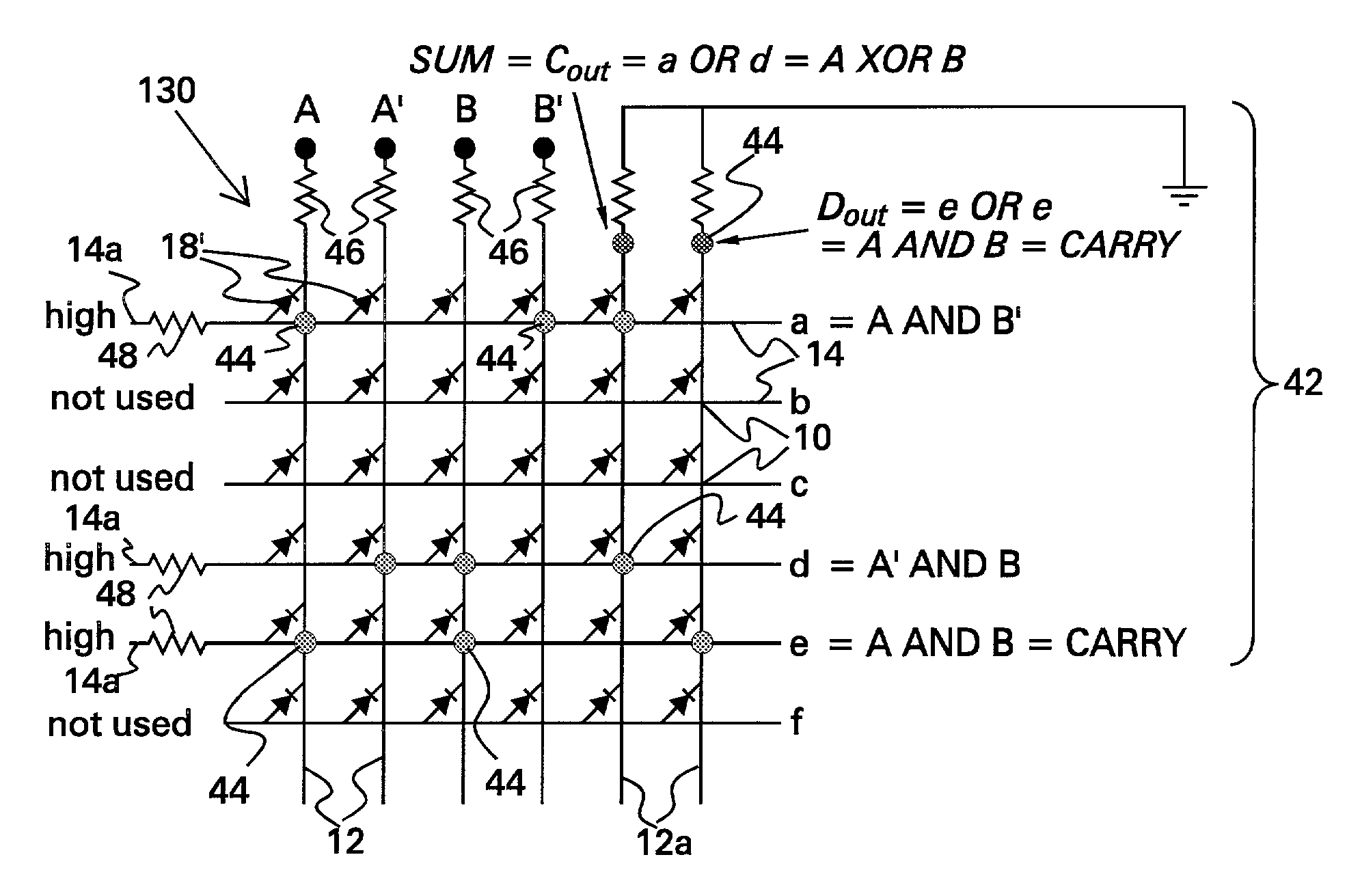
[0065]With only the diode-logic elements described above, a 6×6 diode-crossbar 30, for example, can be turned into a defect-tolerant 2-bit adder 42, as shown in FIG. 7, which uses the logic elements illustrated in FIG. 6A. This logic circuit 42 operates as follows. Certain of the junctions are set to “1”, and these junctions are denoted 44 in FIG. 7. This can be carried out similar to how the crossbar diode memory is configured. These are diode junctions. All other junctions are assumed to have very high resistance and not short the vertical and horizontal wires 12 and 14. Resistors 46 are then connected at the top of the crossbar 30, which may be a relatively long section of nanowire. Additional resistors 48 are connected to the side of the crossbar 30, as needed. This adder uses 4 inputs, labeled A, A′, B, and B′. A and B are the two 1-bit numbers that are to be added together, and A′ and B′ are the complements of those numbers (i.e. if A=“1”, then A′=“0”). Using complements avoid...

example circuit 2

[0066]FIG. 9 depicts the experimentally-determined truth table for an AND gate in which three switches (within a single crossbar) have been configured together to make an AND gate; this device is essentially the same as that shown in FIG. 4B, except that instead of supplying an external resistor, an additional molecular switch was used. It will be noted that in a conventional linear resistor network, even if one had complete control over each resistance value, the best one could hope for in terms of a high / low ratio is a factor of 2, yet the network disclosed herein achieves greater than a factor of 10. This is because the resistors employed in the network of the present invention are based on resonant tunneling through molecules, and the resistance values are voltage-dependent. They are an example of asymmetric non-linear resistors. This allows a much greater voltage difference between logic “0” and logic “1” than can be achieved with linear resistors.

[0067]FIG. 10 depicts the expe...


PUM


Abstract

A programmable logic array (PLA) comprising a two-dimensional array of a plurality of nanometer-scale switches is provided. Each switch comprises a pair of crossed wires which form a junction where one wire crosses another and at least one connector species connecting the pair of crossed wires in the junction. The connector species comprises a bi-stable molecule. A plurality of switches is configurable as an AND gate and a plurality of switches is configurable as an OR gate.

Description

CROSS-REFERENCE TO RELATED APPLICATIONS[0001]The present application is related to the following applications: Ser. No. 09 / 280,189 (“Molecular Wire Crossbar Memory”; now U.S. Pat. No. 6,128,214, issued Oct. 3, 2000); Ser. No. 09 / 280,225 (“Molecular-Wire Crossbar Interconnect (MWCI) For Signal Routing And Communications”; now U.S. Pat. No. 6,314,019, issued Nov. 6, 2001); Ser. No. 09 / 282,049 (“Demultiplexer for a Molecular Wire Crossbar Network (MWCN Demux)”; now U.S. Pat. No. 6,256,767, issued Jul. 3, 2001); Ser. No. 09 / 280,188 (“Molecular Wire Transistor (MWT)”; abandoned, with a first divisional application Ser. No. 09 / 699,080 filed on Oct. 26, 2000, now U.S. Pat. No. 7,030,408, issued Apr. 18, 2006, and a second divisional application Ser. No. 09 / 699,269 filed on Oct. 26, 2000, now U.S. Pat. No. 6,559,468, issued May 6, 2003); and Ser. No. 09 / 282,048 (“Chemically Synthesized and Assembled Electronic Devices”; now U.S. Pat. No. 6,459,095, issued Oct. 1, 2002, with a divisional app...

Claims


Application Information

Patent Timeline
Patent Type & Authority Patents(United States)
IPC IPC(8): H03K19/20H03K19/082
CPCB82Y10/00H01L27/101H01L27/1021H03K19/20H01L29/0665H01L29/0673H01L27/285H10K19/202
Inventor KUEKES, PHILIP J.HEATH, JAMES R.
Owner HEWLETT-PACKARD ENTERPRISE DEV LP
Why Eureka
Try Eureka