

Using crack arrestor for inhibiting damage from dicing and chip packaging interaction failures in back end of line structures
a technology of crack arrestor and back end structure, which is applied in the direction of semiconductor/solid-state device details, semiconductor devices, electrical apparatus, etc., can solve the problems of cracks that damage active areas of chips, chip failure, and uneven density of the material of the dielectric layer, so as to reduce the dielectric constant of the sicoh dielectric material
- Summary
- Abstract
- Description
- Claims
- Application Information
AI Technical Summary
Benefits of technology
Problems solved by technology
Method used
Image

Examples
first preferred embodiment
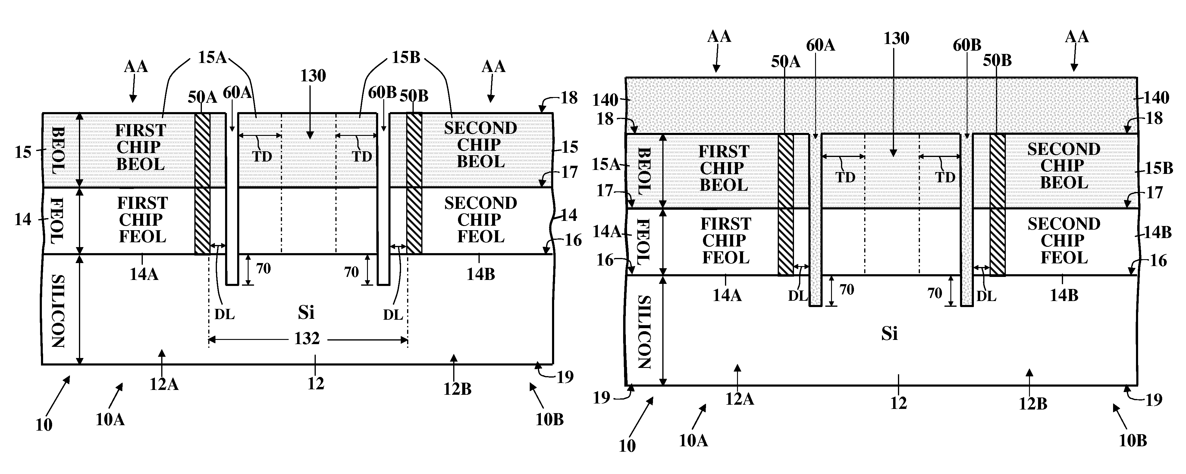
[0087]FIG. 5A is a sectional elevation, taken along line 5A-5A′ in FIG. 4, which shows an enlarged view of the second chip 10B after forming the UDIT 60B located between the edges 110 and the crackstops 50B; and after performing the dicing step in accordance with the process steps of FIG. 10A; but prior to forming an underfill layer 140. As is conventional, the silicon substrate 12B of the second chip 10B is lightly doped. A first FET 22B and a second FET 24B are shown schematically formed in the top surface of the active device layer 14B of the second chip 10B. There are metal interconnects (preferably copper conductors) in the form of horizontally extending metal lines 44 within several stacked dielectric layers 30 in the BEOL structure 15B. As will be well understood by those skilled in the art, the metal interconnects are connected together by the vertically extending metal vias 45. External connections are provided to the FET 22B by the combination of the metal interconnects 42...
second preferred embodiment
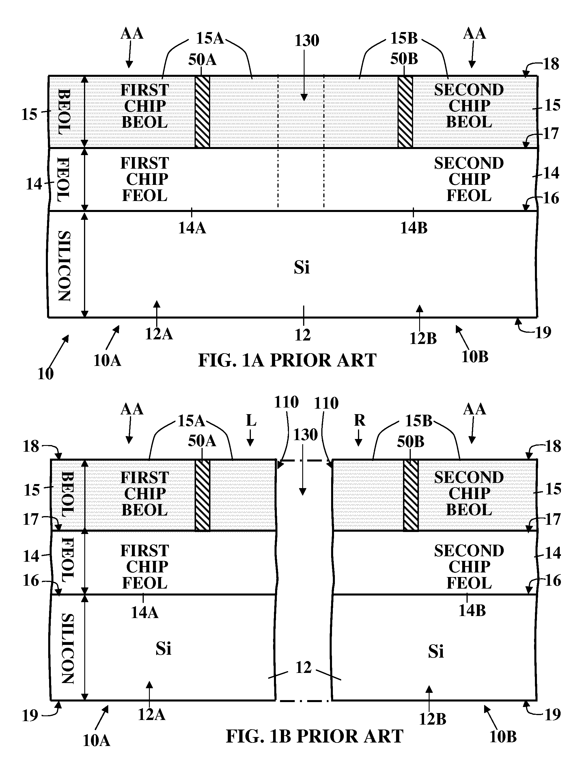
[0096]FIG. 6A shows the device of FIG. 5A with the outer margin 62 indented. i.e. recessed outboard from the UDIT trench between the UDIT trench 60B and the diced edge cut back, thereby forming a recessed region 62A of the BEOL structure 15B in the outer margin 62 thereof. In that portion of the outer margin 62 the interconnect layer 15B has been removed by means such as laser scribe, mechanical saw dicing or other such suitable methods so as to give the structure in FIG. 4 and the chip edge 110. Preferably the recessed region 62A which is located aside from the UDIT trench 60B′ and ILD region 30 has been formed by removing that portion of the BEOL structure 15B down to the top surface of the silicon substrate 12B by a laser ablation process.
[0097]FIG. 6B shows the semiconductor device 10B of FIG. 6A after deposition of the underfill layer 140 and after joining the device to a package 80. The underlayer 140 completely covers the top surface of the BEOL structure 15B and completely f...
third preferred embodiment
[0098]FIGS. 7A, 7B and 7C show sectional views of a modification of the semiconductor device 10B of FIG. 5A in which a plurality of parallel UDIT trenches 60B, 61B and 62B have been formed, between the barrier structure 50B and the chip edge 110. FIG. 7B shows the semiconductor device 10B of FIG. 7A after deposition of the underfill layer 140, completely covering the top surface of the BEOL 15B filling the parallel UDIT trenches 60B, 61B and 62B and after joining the device to a package 80. In the plan view of FIG. 7C, the narrow UDIT trenches 60B, 61B and 62B (which are of equal depth) surrounding the barrier structure 50B and the inner UDIT trenches have successively larger dimensions of length and width as shown in the plan view of FIG. 7C with widths as described above and where the area outside each trench may be intact or removed by previously described processes. An additional benefit of the chip edge in accordance with this invention may be realized once the chip is packaged...
PUM
 Abstract
Description
Claims
Application Information