Organic light emitting device
a light-emitting device and organic technology, applied in the direction of organic semiconductor devices, discharge tube luminescnet screens, natural mineral layered products, etc., can solve the problem that the voltage typically must be increased to achieve a given luminance, and achieve the effect of reducing power consumption, improving driving voltage characteristics, and reducing voltag
- Summary
- Abstract
- Description
- Claims
- Application Information
AI Technical Summary
Benefits of technology
Problems solved by technology
Method used
Image
Examples
example 1
Production of the Organic Light Emitting Device
[0060]For the anode, a Corning 15 Ω / cm2 (1200 Å) ITO glass substrate was cut into a size of 50 mm×50 mm×0.7 mm and washed by sonicating in isopropyl alcohol and deionized water for 5 minutes each, and then treated with UV ozone for 30 minutes.
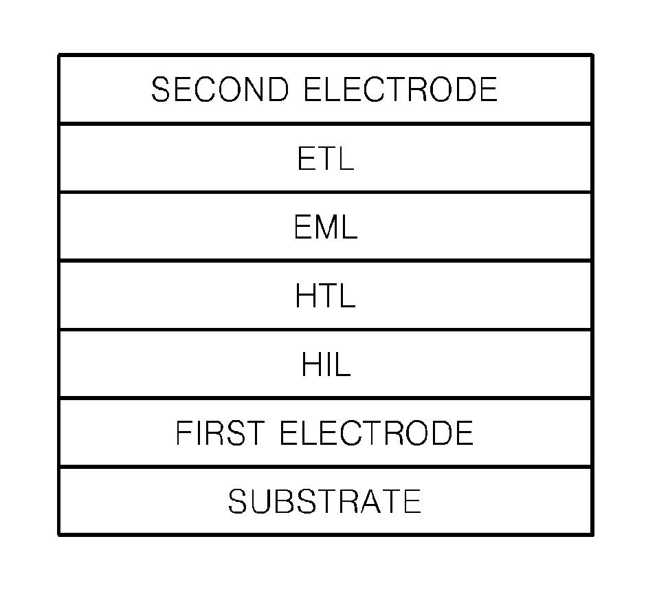
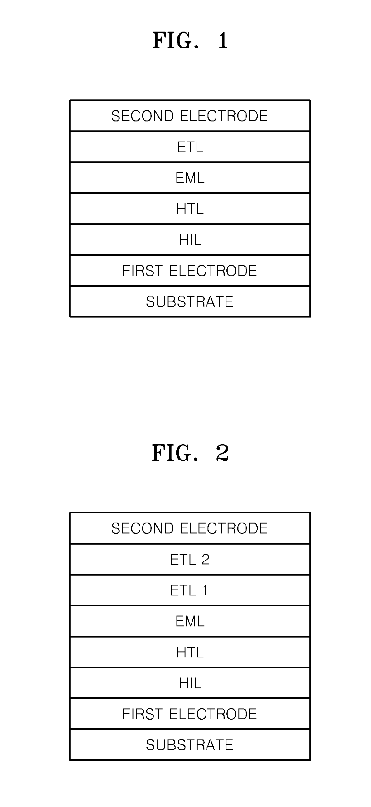
[0061]On the top surface of the substrate, an HIL having a thickness of 5 nm was formed using copper phthalocyanine (CuPc).
[0062]On top of the HIL, an HTL was formed at a thickness of 60 nm by vacuum-depositing N,N′-bis(α-naphthyl)-N,N′-diphenyl-4,4′-diamine (NPB). After forming the HTL as mentioned, an emission layer was formed on top of the HTL by vacuum-depositing 100 parts by weight of Alq3 as a host and 10 parts by weight of coumarin 6 as a dopant.
[0063]Then, an ETL having a thickness of 35 nm was formed by vacuum-depositing 25 parts by weight of LiF and 75 parts by weight of Bebq2 on top of the emission layer.
[0064]Production of the organic light emitting device is completed by vacuum-deposit...
example 2
Production of the Organic Light Emitting Device
[0065]The organic light emitting device was produced in the same manner as in Example 1, except that the ETL was formed by vacuum-depositing 50 parts by weight of lithium quinolate and 50 parts by weight of Bebq2.
example 3
Production of the Organic Light Emitting Device
[0066]For the anode, a Corning 15 Ω / cm2 (1200 Å) ITO glass substrate was cut into a size of 50 mm×50 mm×0.7 mm and washed by sonicating in isopropyl alcohol and deionized water for 5 minutes each, and then washed in UV ozone for 30 minutes.
[0067]On the top surface of the substrate, an HIL having a thickness of 5 nm was formed using copper phthalocyanine (CuPc).
[0068]On top of the HIL, an HTL was formed at a thickness of 60 nm by vacuum-depositing NPB. After forming the HTL as mentioned, an emission layer was formed on top of the HTL by vacuum-depositing 100 parts by weight of Alq3 as a host and 10 parts by weight of coumarin 6 as a dopant.
[0069]Then, a first electron transport layer, ETL1, having a thickness of 10 nm was formed by vacuum-depositing Bebq2 on top of the emission layer.
[0070]A second electron transport layer, ETL2, having a thickness of 15 nm was formed by vacuum-depositing 25 parts by weight of LiF and 75 parts by weight ...
PUM
| Property | Measurement | Unit |
|---|---|---|
| electric field | aaaaa | aaaaa |
| thickness | aaaaa | aaaaa |
| thickness | aaaaa | aaaaa |
Abstract
Description
Claims
Application Information


