Flexible substrate with electronic devices and traces

a flexible substrate technology, applied in the field of electronic devices, to achieve the effect of improving lamination

Inactive Publication Date: 2011-07-12
EASTMAN KODAK CO
View PDF15 Cites 75 Cited by
  • Summary
  • Abstract
  • Description
  • Claims
  • Application Information

AI Technical Summary

Benefits of technology

[0031]It is another advantage of the present invention that it provides a plastic substrate that can offer improved lamination, including self-lamination to a carrier.

Problems solved by technology

Thus, the range of substrate materials that have been used successfully is somewhat limited, generally to glass, quartz, or other rigid, silicon-based materials.
However, problems such as chemical incompatibility between the substrate and TFT materials, thermal expansion mismatch between substrate and device layers, planarity and surface morphology, and capacitive coupling or possible shorting make metal foil substrates less desirable in many applications.
In addition, this capability could enable fabrication of larger displays and devices, since crystalline silicon and many types of glass that are conventionally employed as substrates become increasingly difficult to form and manage in large sheets.
While there are clear advantages to plastic and other flexible substrates, there are significant disadvantages that have discouraged use of such substrates, including the following:Incompatibility with the high temperature range required for TFT fabrication.Poor dimensional stability at high temperatures.Mismatch of coefficient of thermal expansion (CTE) of plastic and thin-film semiconductor materials.High moisture absorption characteristics of plastics.Poor transparency for many types of plastic.The requirement to attach and detach the plastic substrate material from a carrier.
Chief among these disadvantages are temperature-related requirements.
As one alternative solution, U.S. Pat. No. 6,492,026 (Graff et al.) discloses the use of flexible plastic substrates having relatively high glass transition temperatures Tg, typically above 120 degrees C. However, the capability for these substrates to withstand conventional TFT fabrication temperatures much above this range is questionable.
Moreover, in order to use these plastics, considerable effort is expended in protecting the substrate and the device(s) formed from scratch damage and moisture permeation, such as using multiple barrier layers.
Although these and similar solutions have been proposed for forming TFT components on flexible substrates, drawbacks remain.
'442 requires additional fabrication steps and materials and presents inherent alignment difficulties.
'026 disclosure, still leaves thermal expansion (CTE) difficulties and requires additional layers and processes in order to protect the plastic.
'124 disclosures do not provide the full breadth of capabilities of more conventional TFT fabrication techniques and thus have limited utility.
None of these disclosures provide a flexible substrate that truly serves to replace glass or other silicon-based substrate, since the TFT must be formed either on a release layer or on some intermediate layer that must be formed on top of the flexible substrate.
However, even with its advantages, polyimide material presents significant obstacles to direct deposition of TFTs.
The CTE of polyimide differs from that of thin-film semiconductor materials, leading to fracturing and electrical discontinuity following high-temperature fabrication.
However, even where CTE can be more closely matched using microfiller additives, other problems with lamination remain.
Other plastics of interest, such as Teflon®, may have some properties that are more favorable for use as flexible substrates, but present other sets of obstacles that preclude their use with conventional fabrication approaches.
While these approaches are well known for use with multilayer PC boards, however, additional steps would be necessary to attach semiconductor devices to a flexible substrate instead of the conventional PC board material.

Method used


Image

  • Flexible substrate with electronic devices and traces
  • Flexible substrate with electronic devices and traces
  • Flexible substrate with electronic devices and traces

Examples


example 1

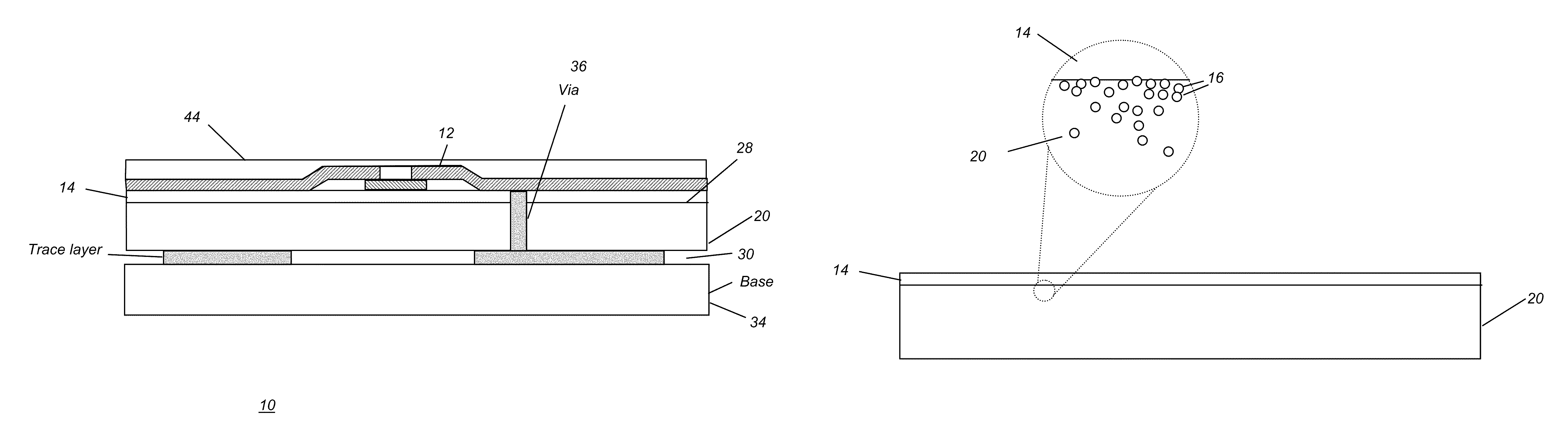
[0069]In one embodiment, the material used for composite substrate 20 is a PTFE woven fiberglass laminate, such as a material from the DiClad 522, 527 Series available from Arlon, Inc. Rancho Cucamonga, Calif. Dimensionally stable under temperature stress, PTFE woven fiberglass laminates have been used, for example, for printed circuit boards (PCBs) and, when used for this purpose, are supplied with a copper layer, typically an electrodeposited copper layer. For use as a flexible substrate 20, an ideal thickness for PTFE woven fiberglass laminate is in the range of about 25 microns to about 3000 microns.

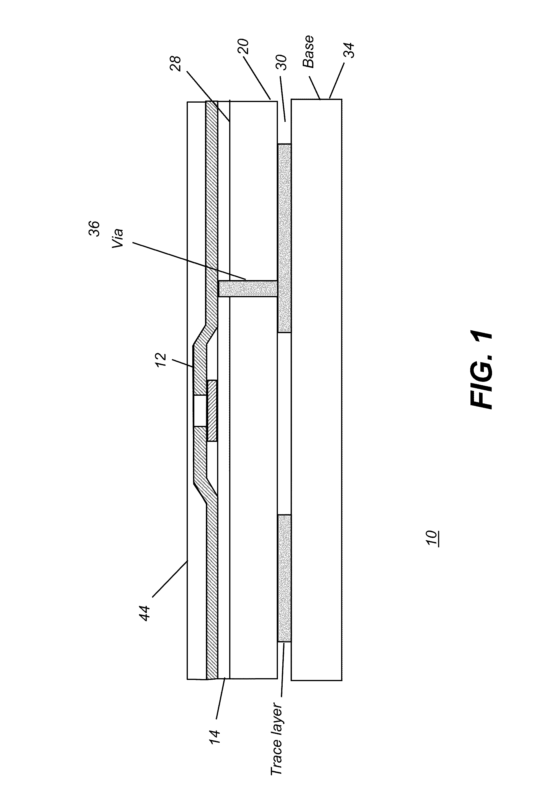
[0070]Given this substrate, TFT fabrication processing is as follows:[0071]1. Mounting on carrier 18. The flexible substrate is initially laminated onto a glass carrier 18. This is done by positioning substrate 20 on carrier 18 and treating this combination by applying heat and pressure to achieve the flow temperature (Tg) of the PTFE material, approximately 300 degrees C. The PTFE m...

example 2

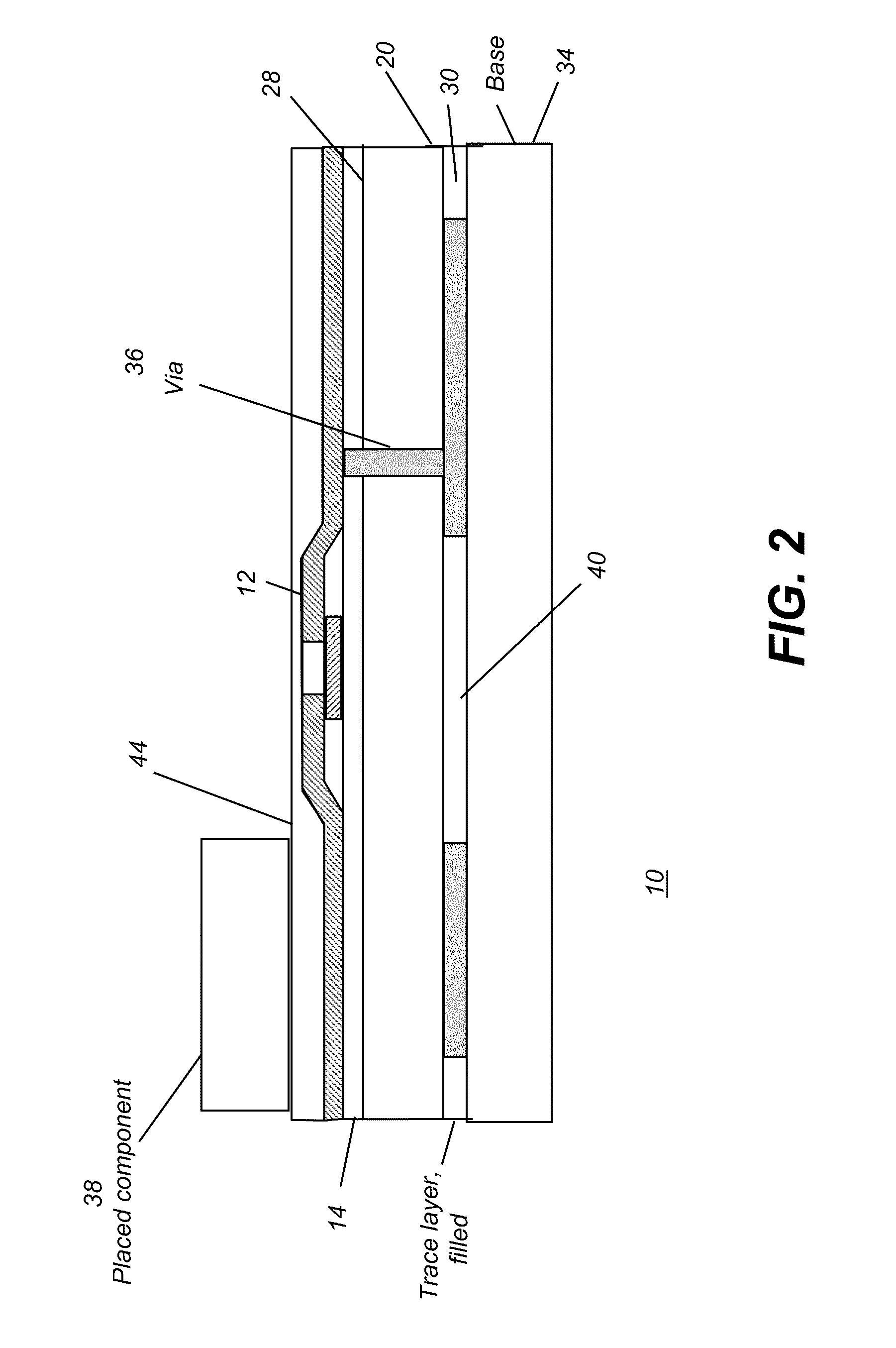
[0082]This next example considers additional steps that may be needed in order to formulate composite substrate 20. The basic steps are as follows:[0083]1. Heat the plastic to its melt temperature Tg.[0084]2. Add particulate material 16 to the melted plastic as a filler. For improved bonding, particulate material 16 works best if deposited on or near the surface of substrate 20. For improved CTE, however, a more general distribution of particles mixed throughout the plastic material is preferred. In most cases, it is preferred to have a thicker concentration of particulate material 16, or exposed portions of particulate material 16 near the surface of substrate 20. Thus, this step would require some mixing of particulate material 16 with the melted plastic binder.[0085]3. Mounting on carrier 18. The flexible substrate is initially laminated onto a glass carrier 18, as is shown in FIG. 7A. This is done by positioning substrate 20 on carrier 18 and treating this combination by applyin...

example 3

[0094]In another embodiment, substrate 20 is formed from polyimide or a polyimide composition and binder, using the following steps:[0095]1. Coat uncured plastic binder material onto a suitable carrier. Here, partially cured polyimide is coated onto the carrier. Any suitable method of application can be used, including dip-skiving, spun-on application, or extrusion.[0096]2. Cure the uncured plastic material until the curing process is largely completed.[0097]3. When approximately 80% of the curing cycle is complete, add particulate material 16 onto the surface of substrate 20. Here, the particulate material 16 is sprinkled onto the surface, to provide an even coating.[0098]4. Complete the curing process, baking off the remaining solvent.[0099]5. Planarization. The desired surface roughness for TFT deposition can be on the order of less than 0.2 to 0.3 microns peak-to-peak in some applications. In order to achieve this, spun-on glass (SOG) is deposited. To apply this substance, a sol...


PUM

PropertyMeasurementUnit
thicknessesaaaaaaaaaa
thicknessaaaaaaaaaa
surface roughnessaaaaaaaaaa

Abstract

A method of manufacturing an electronic device (10) provides a substrate (20) that has a plastic material and has a metallic coating on one surface. A portion of the metallic coating is etched to form a patterned metallic coating. A particulate material (16) is embedded in at least one surface of the substrate. A layer of thin-film semiconductor material is deposited onto the substrate (20).

Description

CROSS REFERENCE TO RELATED APPLICATIONS[0001]Reference is made to commonly-assigned copending U.S. patent application Ser. No. 11 / 461,080, filed Jul. 31, 2006, entitled FLEXIBLE SUBSTRATE WITH ELECTRONIC DEVICES FORMED THEREON, by Tredwell at al., the disclosure of which is incorporated herein.FIELD OF THE INVENTION[0002]This invention generally relates to electronic devices and more particularly relates to an electronic device and its interconnect traces fabricated on a flexible substrate.BACKGROUND OF THE INVENTION[0003]Thin-film transistor (TFT) devices are widely used in switching or driver circuitry for electro-optical arrays and display panels. TFT devices are conventionally fabricated on rigid substrates, typically glass or silicon, using a well-known sequence of deposition, patterning and etching steps. For example, amorphous silicon TFT devices require deposition, patterning, and etching of metals, such as aluminum, chromium or molybdenum, of amorphous silicon semiconductor...

Claims


Application Information

Patent Timeline
Patent Type & Authority Patents(United States)
IPC IPC(8): H01L21/00H01L21/84H01L21/44H01L21/469H01L21/31
CPCH01L29/78603H01L27/124Y10T156/10
Inventor TREDWELL, TIMOTHY J.KERR, ROGER S.
Owner EASTMAN KODAK CO
Why Eureka
Try Eureka