
Semiconductor device and method for manufacturing the same
a technology of metallic oxide film and semiconductor, which is applied in the direction of semiconductor devices, basic electric elements, electrical equipment, etc., can solve the problems of reduced yield, easy reduction of yield, and inability to control the threshold voltage (vth) of tft in subsequent processes, so as to reduce the distribution of oxide fet, improve the characteristics of oxide fet, and reduce yield
- Summary
- Abstract
- Description
- Claims
- Application Information
AI Technical Summary
Benefits of technology
Problems solved by technology
Method used
Image

Examples
first embodiment
Configuration and Manufacturing Method
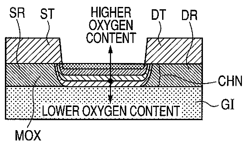
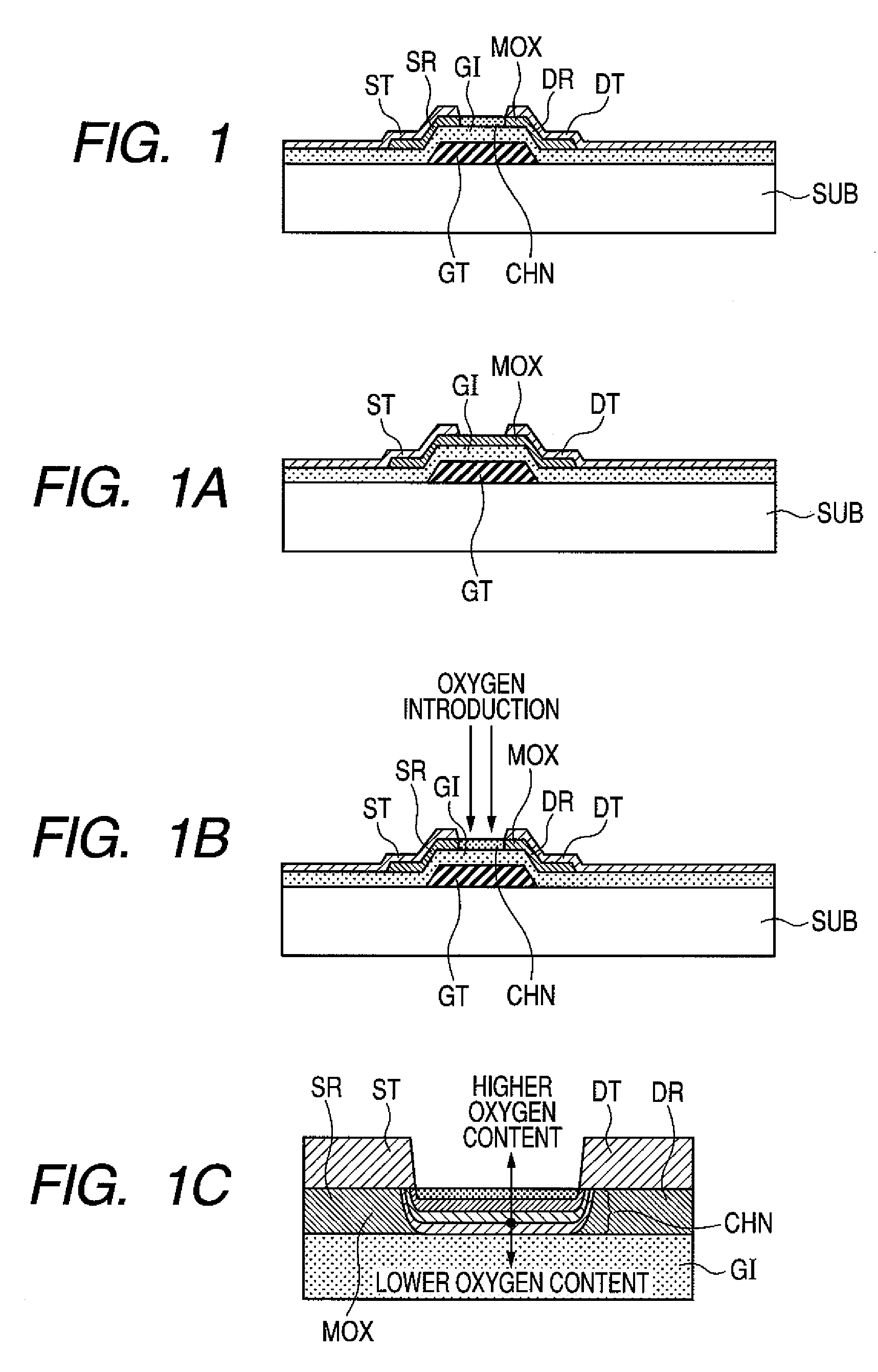
[0053]FIG. 1 is a configuration illustrating the first embodiment of a semiconductor device according to the present invention. A so-called bottom-gate type oxide TFT is shown as a semiconductor device. As shown in FIG. 1, a gate electrode GT is formed over a substrate SUB. Then, a gate insulator film GI is formed over the top surface of the substrate SUB covering the aforementioned gate electrode GT. In addition, a metallic oxide film MOX is formed over the aforementioned gate insulator film GI extending over at least the aforementioned gate electrode GT. Moreover, a source electrode ST and a drain electrode DT are formed directly in contact with the aforementioned metallic oxide film MOX. The source electrode ST and the drain electrode DT are separated on at least the gate electrode GT and formed opposing each other and existing between this separation part. Herein, the aforementioned metallic oxide film MOX consists of a channel region CHN in...
second embodiment
Configuration and Manufacturing Process
[0065]FIG. 5 is cross-sectional drawings illustrating the second embodiment of the semiconductor device in the present invention. FIG. 5 is drawings where two kinds of bottom-gate type oxide TFTs with different Vth are formed over the same substrate.
[0066]That is, the oxide TFT 1 and the oxide TFT 2 are formed over the top surface of the substrate SUB 1. These oxide TFT 1 and oxide TFT 2 have almost the same stacking structure of the material layers constituting them; the Vth is made higher in the oxide TFT 1; and the Vth is made lower in the oxide TFT 2. That is, the oxygen content introduced into the oxide TFT 1 is made higher than that in the source region SR and the drain region DR in the channel region CHN, and the oxide TFT 2 is formed to have no oxygen content difference from the source region SR and the drain region DR in the channel region CHN.
[0067]FIGS. 5A and 5B are explanatory drawings illustrating a manufacturing method of a semic...
third embodiment
Configuration and Manufacturing Process
[0070]FIG. 6 is cross-sectional drawings illustrating the third embodiment of the semiconductor device in the present invention and they are drawings corresponding to FIG. 5. As well as the case of FIG. 5, FIG. 6 is drawings where two kinds of bottom-gate type oxide TFTs with different Vth are formed over the same substrate. The configuration which is different from the case of FIG. 5 is that oxygen is introduced into the channel region CHN in the oxide TFT 2 and the content thereof is made lower than the oxygen content of the channel region CHN in the oxide TFT 1.
[0071]FIGS. 6A and 6B are explanatory drawings illustrating a manufacturing method of a semiconductor device shown in FIG. 6. First of all, the oxide TFT 1 and the oxide TFT 2 are formed to be the structure shown in FIG. 1B by using a general manufacturing process and the manufacturing process disclosed in this specification (FIG. 6A). At this stage, the same amount of oxygen is intro...
PUM
| Property | Measurement | Unit |
|---|---|---|
| metallic | aaaaa | aaaaa |
| conductivity | aaaaa | aaaaa |
| threshold voltage | aaaaa | aaaaa |
Abstract
Description
Claims
Application Information