
Method for manufacturing semiconductor optical device

a semiconductor optical and manufacturing method technology, applied in semiconductor lasers, semiconductor/solid-state device testing/measurement, instruments, etc., can solve the problems of blue-violet ld operating voltage rise, contact resistance might be elevated, process freedom or the like lowered, etc., to achieve the effect of preventing the decrease of the contact area and simple steps

Inactive Publication Date: 2011-07-19
MITSUBISHI ELECTRIC CORP
View PDF20 Cites 4 Cited by
  • Summary
  • Abstract
  • Description
  • Claims
  • Application Information

AI Technical Summary

Benefits of technology

[0024]The present invention has been made to solve the problem, and the first object of the present invention is to provide a method for manufacturing a semiconductor optical device at a high yield by simple steps that can stably prevent decrease in the contact area between a semiconductor layer and an electrode layer on the upper surface of a waveguide ridge, and damages in the semiconductor layer on the top of the waveguide ridge by etching.
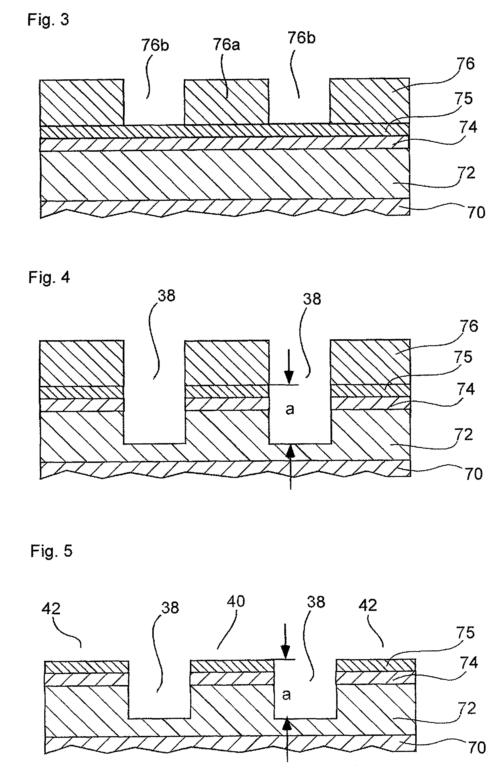
[0026]Accordingly, in the method for manufacturing a semiconductor optical device according to the present invention, the second resist pattern formed in the dent adjoining the waveguide ridge has a surface higher than the surface of the cap layer of the waveguide ridge, but lower than the surf ace of the insulating film on the top of the waveguide ridge. When the insulating film on the top of the waveguide ridge is removed by dry etching using the second resist pattern, the cap layer on the top of the waveguide ridge is exposed leaving the insulating film on the side of the waveguide ridge and in the dent. Furthermore, when the cap layer is removed by wet etching, the second semiconductor layer is exposed, and an electrode layer is formed on the exposed second semiconductor layer. Therefore, the second semiconductor layer can be joined to the electrode layer without the shrinkage of the contact area. And since the cap layer has been formed on the second semiconductor layer of the waveguide ridge when the insulating film by dry etching using the second resist pattern as the mask is removed, the damage of the second semiconductor layer due to dry etching can be prevented, and the elevation of the contact resistance of the second semiconductor layer caused by dry etching can be suppressed.
[0028]Accordingly, in the method for manufacturing a semiconductor optical device according to the present invention, the electrode layer can be joined to the second semiconductor layer without the shrinkage of the contact area. Furthermore, since no dry etching is used when the second semiconductor layer on the top of the waveguide ridge is exposed, no damages due to dry etching occur in the second semiconductor layer, and the elevation of the contact resistance can be suppressed.
[0030]Accordingly, in the method for manufacturing a semiconductor optical device according to the present invention, the second resist pattern formed in the dent adjoining the waveguide ridge has a surface higher than the surface of the cap layer of the waveguide ridge, but lower than the surface of the insulating film on the top of the waveguide ridge. When the insulating film on the top of the waveguide ridge is removed by dry etching using the second resist pattern, the cap layer on the top of the waveguide ridge is exposed leaving the insulating film on the side of the waveguide ridge and in the dent. Furthermore, when the cap layer is removed by wet etching, the second semiconductor layer is exposed, and an electrode layer is formed on the exposed second semiconductor layer. Therefore, the second semiconductor layer can be joined to the electrode layer without the shrinkage of the contact area. And since the cap layer has been formed on the second semiconductor layer of the waveguide ridge when the insulating film by dry etching using the second resist pattern as the mask is removed, the damage of the second semiconductor layer due to dry etching can be prevented, and the elevation of the contact resistance of the second semiconductor layer caused by dry etching can be suppressed.
[0032]Accordingly, in the method for manufacturing a semiconductor optical device according to the present invention, the electrode layer can be joined to the second semiconductor layer without the shrinkage of the contact area. Furthermore, since no dry etching is used when the second semiconductor layer on the top of the waveguide ridge is exposed, no damages due to dry etching occur in the second semiconductor layer, and the elevation of the contact resistance can be suppressed.

Problems solved by technology

However, in the case of a blue-violet LD, since the material used in the contact layer is GaN or the like, and the contact resistance of the material is relatively high, decrease in the contact area between the electrode and the contact layer elevated the contact resistance between the electrode and the contact layer, resulting in the elevation of the operating voltage of the blue-violet LD.
By these conventional methods, even if the contact area between the contact layer and the electrode layer of the waveguide ridge is secured, there were problems in stably manufacturing a device having all favorable characteristics, such as the step for simultaneously etching the metal film and the semiconductor layer under the metal film; the step for discontinue etching stably leaving a predetermined thickness of the underlying resist when two layers of resist were used; and the step performing liftoff when a metal film was used as the mask or a plurality of protective films were used.
There were also problems of the lowering of process freedom or the like when a plurality of resists or protective films were used.
For example, when the underlying layer of the SiO2 film was a p-type contact layer, it might be damaged by etching, and contact resistance might be elevated.
Especially when the p-type contact layer was composed of a material containing GaN, there was a problem in that it was difficult to remove the material containing GaN by wet etching, and it was difficult to remove the damaged portion by wet etching.

Method used


Image

  • Method for manufacturing semiconductor optical device
  • Method for manufacturing semiconductor optical device
  • Method for manufacturing semiconductor optical device

Examples


first embodiment

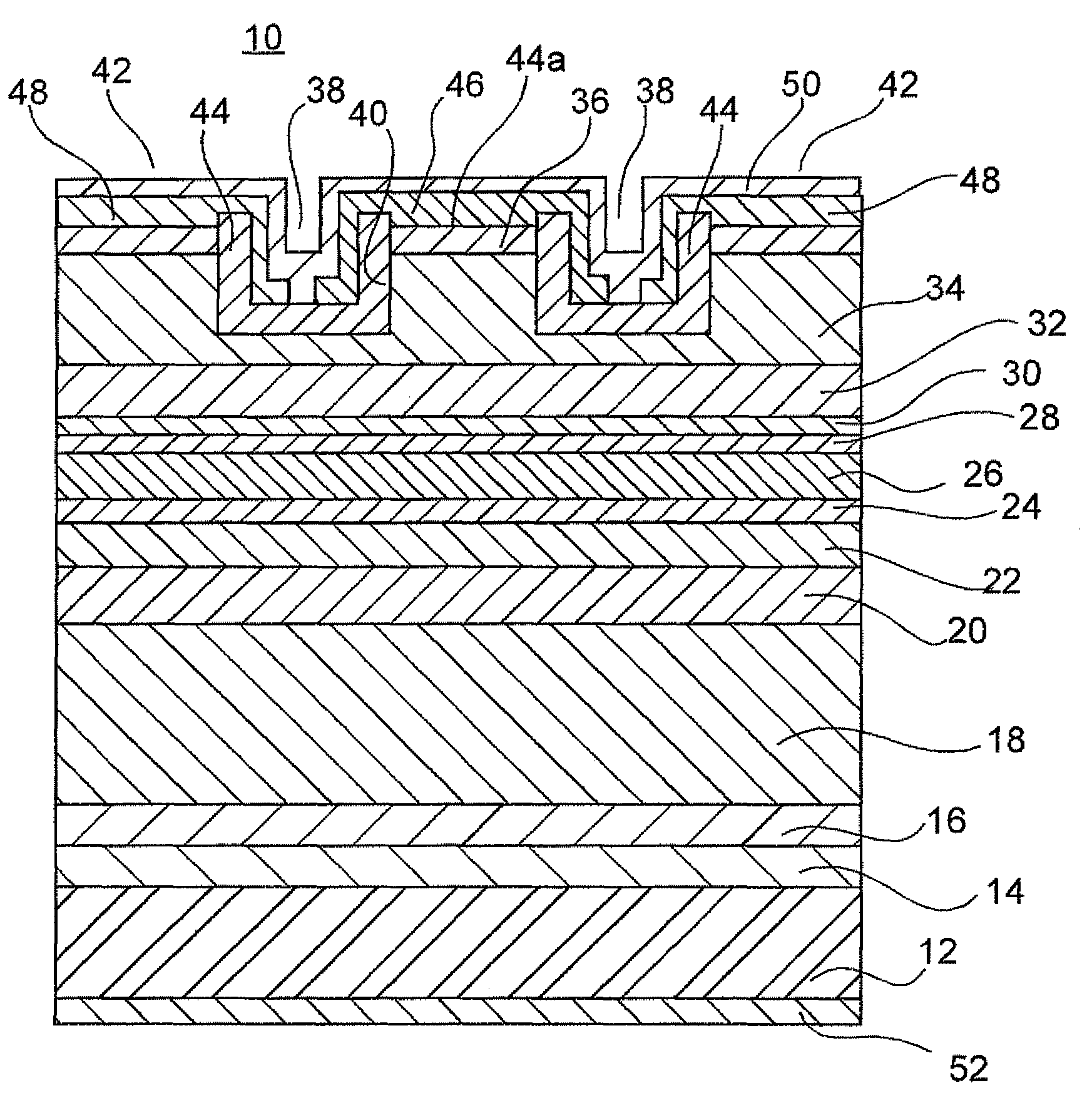
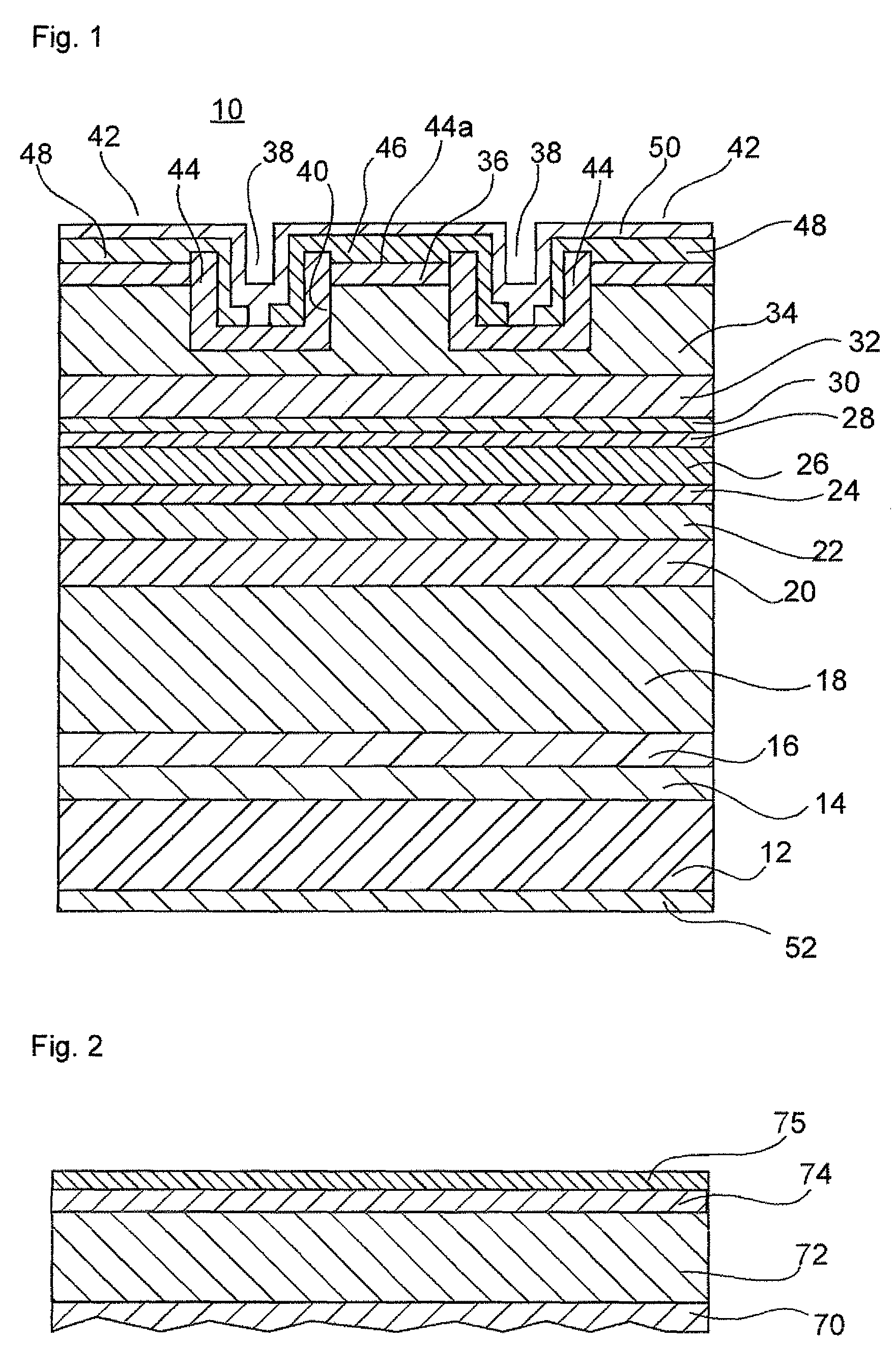
[0042]FIG. 1 is a sectional view showing a semiconductor LD according to an embodiment of the present invention. In the drawings herein, the same numerals and characters denote the same or equivalent parts.

[0043]In FIG. 1, the LD 10 is a blue-violet LD of a waveguide ridge type, wherein a buffer layer 14 formed on the Ga surface, which is a major surface of n-type GaN substrate 12 (hereafter “n-type” is simply referred to as “n-”, “p-type” is simply referred to as “p-”, and in the case of “undoped” wherein no impurities are doped is simply referred to as “i-”), for example, a first n-clad layer 16, a second n-clad layer 18, and a third n-clad layer 20 as first semiconductor layers formed of n-AlGaN are formed on the buffer layer 14; and an n-side light guiding layer 22 formed of n-GaN, an n-side SCH (separate confinement hetero-structure) layer 24 formed of InGaN, and an active layer 26 are sequentially laminated on the third n-clad layer 20.

[0044]On the active layer 26 are sequenti...

first modification

[0110]FIGS. 15 to 17 are partially sectional views illustrating each manufacturing step on another method for manufacturing a semiconductor LD according to the present invention.

[0111]Among manufacturing steps described above, steps shown in FIGS. 1 to 6 are same also in the first modification. The steps shown in FIGS. 7 and 8 in the above description are substituted by the steps shown in FIGS. 15 to 17.

[0112]In the step shown in FIG. 6, after the upper surface of the waveguide ridge 40, the inner surfaces of channels 38, and the upper surface of the electrode pad base 42 have been coated by the SiO2 film 78, referring to FIG. 15, a photo-resist mainly consisting of a novolak resin is applied onto the entire surface of the wafer to form a resist film 90 wherein the surface thereof in channels 38 adjoining the waveguide ridge 40 has the substantially same height as the upper surface of the SiO2 film 78.

[0113]In this embodiment, the thickness d of the resist film 90 in the channels 38...

second embodiment

[0132]FIG. 18 is a sectional view of a semiconductor LD according to an embodiment of the present invention.

[0133]In FIG. 18, the LD 100 if a blue-violet LD of a waveguide ridge type, and has a configuration substantially the same as the configuration of the LD 10 described in the first embodiment.

[0134]The difference of the LD 100 from the LD 10 is that the both side and bottoms of the channels 38 including the sidewalls of the waveguide ridge 40 and the electrode pad base 42 are coated with the first silicon oxide film 44 in the LD 10; however, the both sides of the channels 38 including the sidewalls of the waveguide ridge 40 and the electrode pad base 42 are not coated with the first silicon oxide film 44, and only the bottoms of the channels 38 are coated with the first silicon oxide film 44 in the LD 100.

[0135]Therefore, the p-side electrode 46 directly contacts the upper surface of the contact layer 36 and the sidewalls of the waveguide ridge 40, and extends to the bottoms of...


PUM


Abstract

After a metal cap layer is laminated on a semiconductor laminated structure, a waveguide ridge is formed, the waveguide ridge is coated with an SiO2 film, and a resist is applied; then, a resist pattern is formed, the resist pattern exposing the surface of the SiO2 film on the top of the waveguide ridge, and burying the SiO2 film in channels with a resist film having a surface higher than the surface of the metal cap layer of the waveguide ridge and lower than the surface of the SiO2 film of the waveguide ridge; the SiO2 film is removed by dry etching, using the resist pattern as a mask. The metal cap layer is removed by wet etching, and a p-GaN layer of the waveguide ridge is exposed to form the electrode layer.

Description

BACKGROUND OF THE INVENTION[0001]1. Field of the Invention[0002]The present invention relates to a method for manufacturing a semiconductor optical device, and more specifically to a method for manufacturing a semiconductor optical device having an electrode on the top of a waveguide ridge.[0003]2. Description of the Related Art[0004]In recent years, as a semiconductor laser that can emit light from a blue region to a violet region required in high-density optical disks, a nitride semiconductor laser using a III-V nitride compound semiconductor, such as AlGaInN, has been actively studied and developed, and has been already put in practical use.[0005]Such a blue-violet laser diode (hereafter, a laser diode will be abbreviated as an LD) is formed by growing the crystals of a compound semiconductor on a GaN substrate.[0006]Typical compound semiconductors include III-V compound semiconductors wherein a group III element is combined with a group V element, and by combining a plurality of...

Claims


Application Information

Patent Timeline
Patent Type & Authority Patents(United States)
IPC IPC(8): H01L21/00
CPCB82Y20/00H01S5/0425H01S5/22H01S5/2009H01S5/2214H01S5/34333H01S5/04254H01S5/04252H01S2301/176
Inventor ABE, SHINJIKAWASAKI, KAZUSHIGE
Owner MITSUBISHI ELECTRIC CORP
Learn More