Circuit board with embedded component and method of manufacturing same

a technology of embedded components and circuit boards, which is applied in the association of printed circuit non-printed electrical components, semiconductor/solid-state device details, and electrical apparatus construction details, etc. it can solve the problems of increasing the complexity of the wiring pattern on the surface of the wiring pattern and the number of electrical connections between the surfaces, increasing the number of via holes to be formed, and reducing the number of circuit boards. , to achieve the effect of shortening the connection length, improving the electrical characteristics of the circuit board,

Inactive Publication Date: 2011-08-02
LAPIS SEMICON CO LTD
View PDF23 Cites 13 Cited by
  • Summary
  • Abstract
  • Description
  • Claims
  • Application Information

AI Technical Summary

Benefits of technology

[0012]An object of the present invention is to increase the mounting density of circuit boards with embedded components.
[0015]A still further object is to improve the productivity of the circuit board manufacturing process.
[0021]When a conductor on the surface of an electronic component embedded in a circuit board must be electrically connected to a point on the distant surface of the substrate or prepreg on which the electronic component is mounted, routing the connection through a hole in the electrical component itself as described above saves space and shortens the length of the connection, thereby improving the electrical characteristics of the circuit board and enabling components to be more densely mounted.
[0022]By using prepregs with openings accommodating the embedded electronic component, the invented methods of manufacturing the circuit board simplify the manufacturing process and improve productivity.

Problems solved by technology

As the complexity of the semiconductor devices mounted on circuit boards increases year by year, the complexity of the wiring patterns on their surfaces and the number of electrical connections necessary between the surfaces also increases, requiring a large number of via holes to be formed.
The embedding of WCSP components in such a circuit board is subject to layout constraints, not only because the embedded WCSP components must avoid the numerous via holes, but also because the embedded WCSP components require the formation of additional via holes for electrical connections that pass between the two surfaces of the circuit board as illustrated in FIG. 4.
These constraints pose another problem; if they could be partially removed, additional layout space could be obtained and the component mounting density could be increased.

Method used


Image

  • Circuit board with embedded component and method of manufacturing same
  • Circuit board with embedded component and method of manufacturing same
  • Circuit board with embedded component and method of manufacturing same

Examples


first embodiment

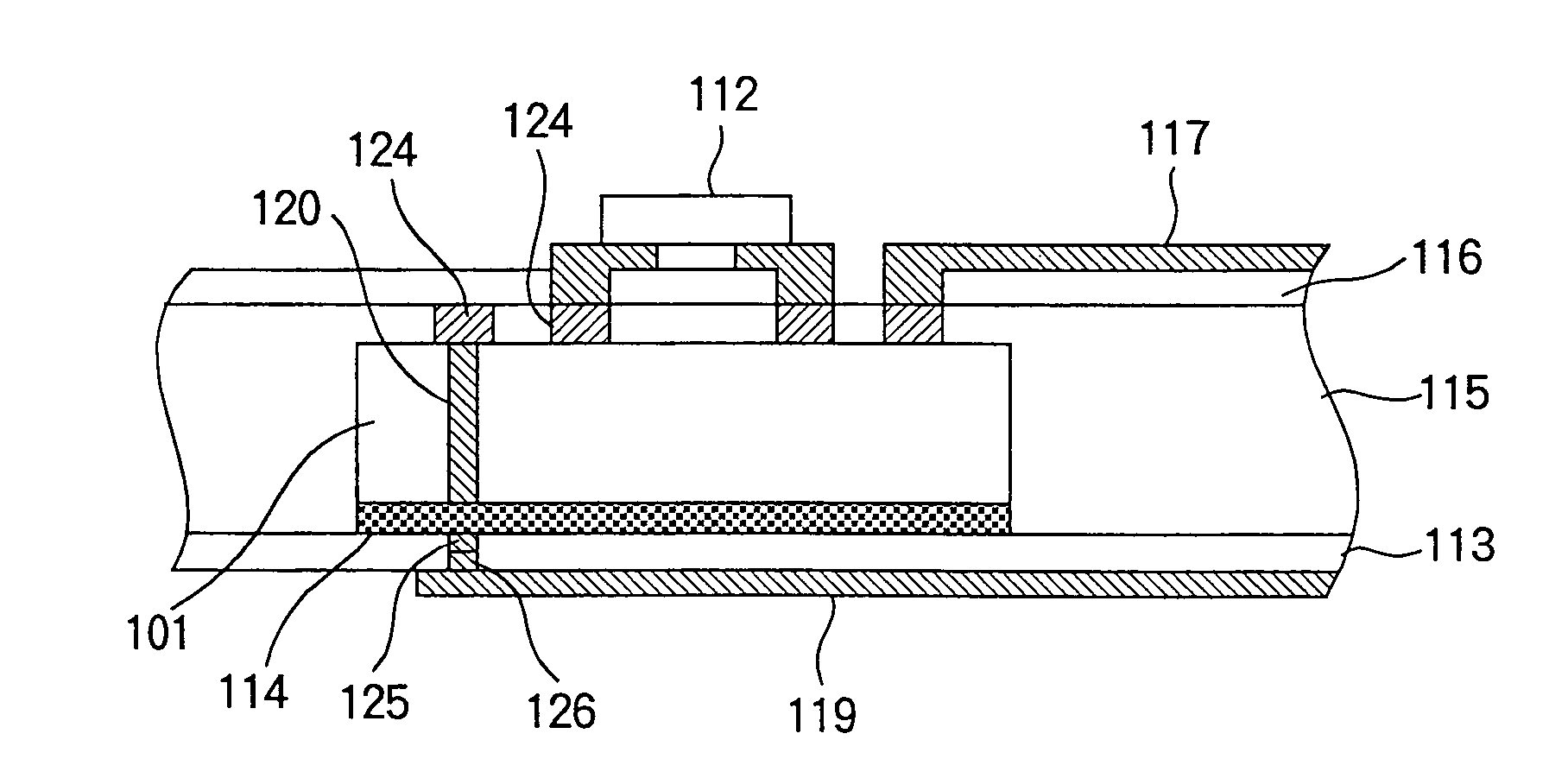
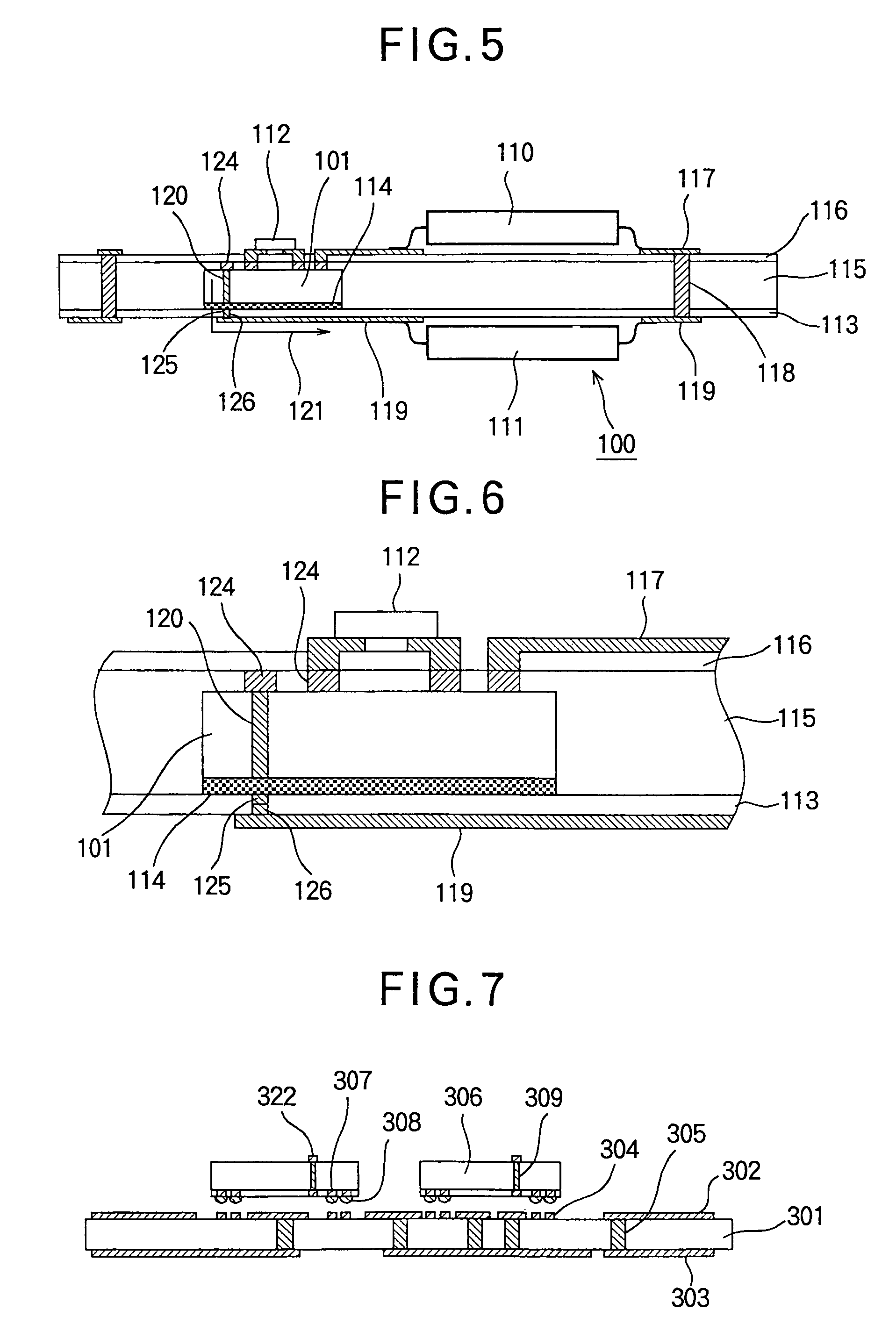
[0031]Referring to FIG. 5, a circuit board 100 in the first embodiment of the invention includes an embedded WCSP component 101, semiconductor devices 110, 111, and a chip component 112.

[0032]The embedded WCSP component 101 is attached to a substrate 113 by means of a die bonding adhesive 114 and is sealed with a dielectric layer 115 on which a further dielectric layer 116 is formed. The two dielectric layers 115, 116 may be formed simultaneously as a single layer. The embedded WCSP component 101 is an integrated circuit with circuit elements and interconnections (not shown) disposed near the upper surface in the drawing.

[0033]Dielectric layer 116 forms the first surface of the circuit board 100, on which semiconductor device 110 and chip component 112 are mounted. The undersurface of the substrate113 forms the second surface of the circuit board 100, on which semiconductor device 111 is mounted. Semiconductor device 110 and chip component 112 make electrical contact with a wiring p...

second embodiment

[0038]The invention can also be practiced in multi-layer circuit boards. FIGS. 7 to 10 show steps in the fabrication of a four-layer circuit board 300 including a pair of embedded WCSP components 306.

[0039]Referring to FIG. 7, a substrate 301 is prepared. The substrate 301 has two major surfaces: a first surface on which a wiring pattern 302 and a plurality of electrode pads 304 are formed, and a second surface, opposite the first surface, on which a wiring pattern 303 is formed. The substrate 301 additionally has conductors 305 disposed in holes extending through the substrate 301 from the first surface to the second surface. Each WCSP component 306 has a first surface on which a plurality of electrode pads 307 and external terminals 308 are formed, and a second surface, opposite the first surface, on which an electrode pad 322 is formed. A hole extends through each WCSP component 306 from the first surface to the second surface. A conductor 309 is formed in this hole, electrically...

third embodiment

[0048]The prepreg method illustrated in the second embodiment can also be used to fabricate a circuit board of the type described in the first embodiment. As a third embodiment of the invention, FIGS. 11 to 14 show steps in the fabrication of such a circuit board 400 including an embedded WCSP component 101.

[0049]Referring to FIG. 11, the WCSP component 101 has the structure described in the first embodiment, with a conductor 120 in a hole electrically connecting one of a plurality of electrode pads 124 formed on one major surface to an electrode pad 125 formed on the other major surface.

[0050]As in the second embodiment, three prepregs are prepared: a first prepreg 405 clad on one surface with copper foil 406, a second prepreg 403 having an opening 404 for the WCSP component 101, and a third prepreg 402 clad on one surface with copper foil 401.

[0051]Referring to FIG. 12, the WCSP component 101 is attached to the unclad surface of the first prepreg 405 by a die bonding adhesive 114....


PUM

PropertyMeasurementUnit
sizeaaaaaaaaaa
densityaaaaaaaaaa
conductiveaaaaaaaaaa

Abstract

A circuit board has an embedded electronic component such as an integrated circuit chip with a wafer level chip size package. A via hole extends through the electronic component. Another via hole extends through the substrate or prepreg on which the electronic component is mounted inside the circuit board. Conductors in the via holes enable a terminal on the surface of the electronic component to be electrically connected to a wiring pattern or another electronic component on the opposite side of the substrate or prepreg. Routing the connection through the electronic component itself saves space and reduces the length of the connection.

Description

BACKGROUND OF THE INVENTION[0001]1. Field of the Invention[0002]The present invention relates to a printed circuit board having an embedded electronic component with a via hole.[0003]2. Description of the Related Art[0004]It is known technology to embed passive electronic components such as resistors and capacitors and active electronic components such as integrated circuit chips in a printed circuit board, to increase the mounting density of the board. Embedded integrated circuit chips must have small packages, so it is advantageous to use chip scale packages, which are barely larger than the integrated circuit chip itself, or chip size packages, which in plan view are the same size as the chip itself. Recently, wafer level chip size packages have become prevalent. A wafer level chip size package (WCSP) is simply a dielectric layer covering the chip surface on which the integrated circuit is created, with conductive terminals such as solder bumps providing electrical access to the ...

Claims


Application Information

Patent Timeline
Patent Type & Authority Patents(United States)
IPC IPC(8): H05K3/36H05K1/16H05K3/30H05K3/20H05K1/11H05K7/00H05K1/18H01K3/10
CPCH01L24/19H05K1/185H05K1/186H01L24/24H01L23/5389H01L23/49816Y10T29/49131H01L2224/04105H01L2224/20H01L2224/211H01L2224/92244H01L2924/01029H01L2924/14H01L2924/19041H01L2924/19043H01L2924/01005H01L2924/01006H01L2924/01033H01L2924/014H01L2224/16225H01L2224/32225H01L2224/73204Y10T29/49165Y10T29/49133Y10T29/4913H01L2224/0401H01L2224/2518Y10T29/49126Y10T29/49128H01L2924/00H01L2924/15787
Inventor SHIZUNO, YOSHINORI
Owner LAPIS SEMICON CO LTD
Why Eureka
Try Eureka