Method for manufacturing light-emitting device

a technology of light-emitting devices and manufacturing methods, which is applied in the direction of identification means, instruments, vacuum evaporation coatings, etc., can solve the problems of poor film quality and high risk of uneven film formation in this manner, and achieve high light-emitting characteristics, high accuracy, and high definition

Inactive Publication Date: 2011-08-09
SEMICON ENERGY LAB CO LTD
View PDF22 Cites 14 Cited by
  • Summary
  • Abstract
  • Description
  • Claims
  • Application Information

AI Technical Summary

Benefits of technology

[0013]Therefore, an object of one embodiment of the present invention is to provide a method for manufacturing a light-emitting device with high definition, high light-emitting characteristics, and the long lifetime by applying a method in which a desired evaporation pattern can be formed and an excess evaporation of a material layer which is to be the transfer layer is prevented and in which deterioration of the material or the like is hard to occur in a transfer step.
[0025]Light irradiation is performed twice in the method for manufacturing a light-emitting device related to one embodiment of the present invention, which enables pattern formation of the material layer over the evaporation donor substrate and deposition of the material layer onto the deposition target substrate. Specifically, the material layer formed over the evaporation donor substrate is patterned by the first light irradiation and the patterned material layer is evaporated onto the deposition target substrate by the second light irradiation, whereby the material layer can be evaporated with high accuracy. Therefore, the light-emitting device with high definition, high light-emitting characteristics, and the long lifetime can be manufactured.
[0026]Note that, since a light source which emits light having high intensity instantaneously is used in first light irradiation, irradiation time can be shortened and can prevent deformation of a pattern region due to heat conduction. Further, since the material layer over the evaporation donor substrate is patterned in the first light irradiation, a light source which emits light with lower intensity than that in the first light irradiation can be used in the second light irradiation regardless of heat conduction. Accordingly, deterioration of the material layer evaporated onto the deposition target substrate due to light irradiation can be prevented.
[0027]Note that, when lamp light is used as a light source in the second light irradiation, since a film can be deposited on a large area at one time, productivity of a light-emitting device can be improved. Further, in the present invention, by heating the evaporation donor substrate indirectly or directly instead of the second light irradiation, the evaporation material over the evaporation donor substrate may be sublimated and deposited onto the deposition target substrate.

Problems solved by technology

Further, after the transfer, the resulting film formed in this manner is likely to be very uneven and poor in its film quality.

Method used


Image

  • Method for manufacturing light-emitting device
  • Method for manufacturing light-emitting device
  • Method for manufacturing light-emitting device

Examples


embodiment 1

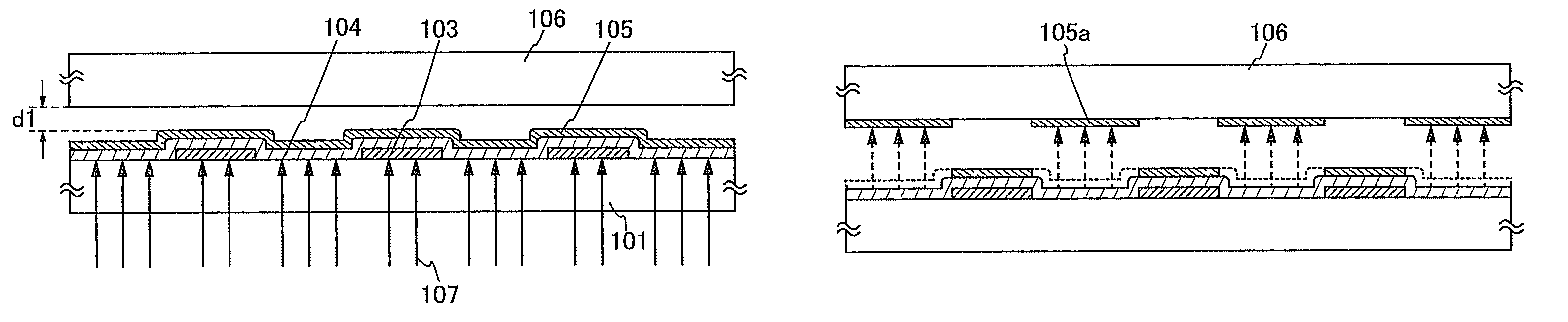
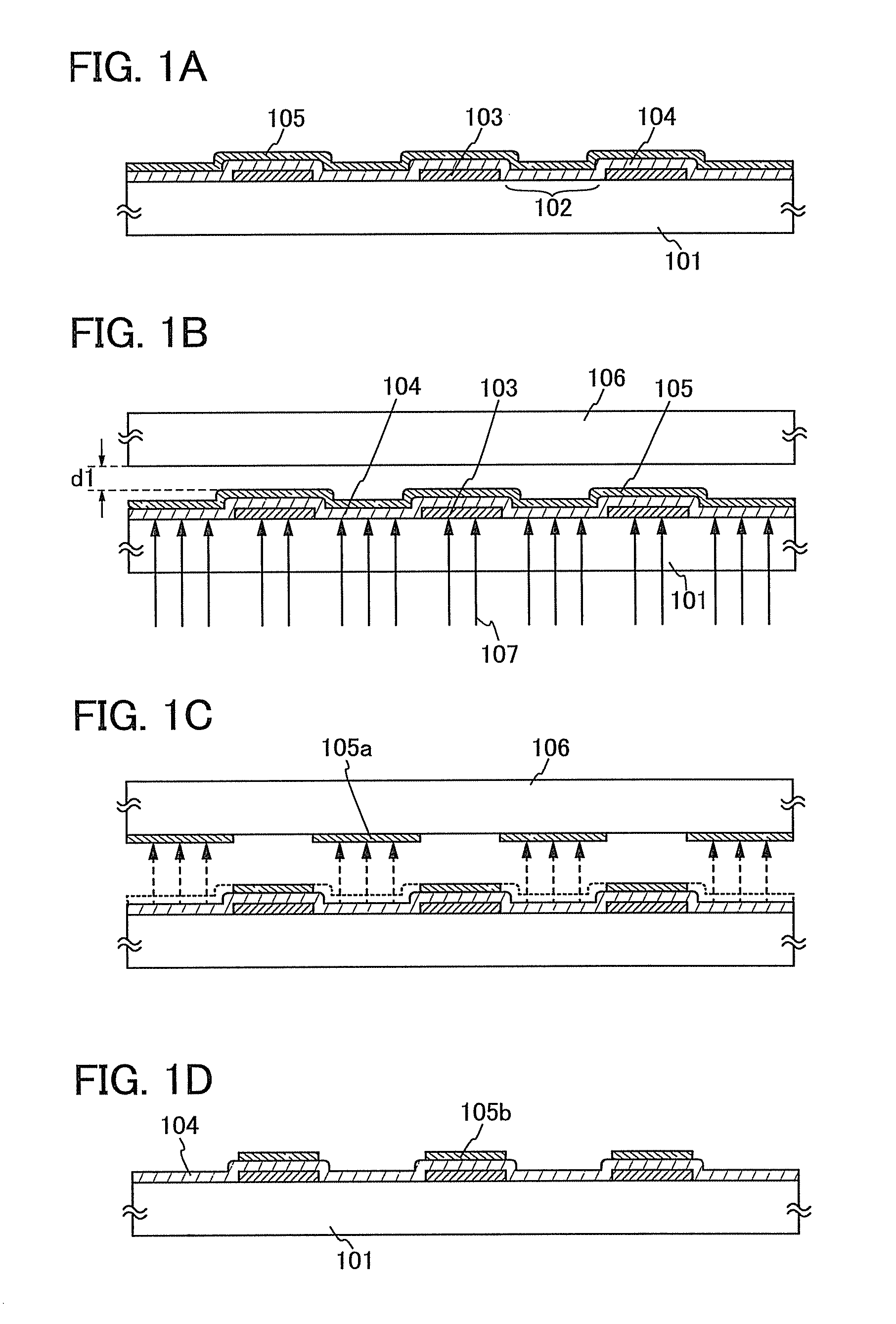
[0043]Embodiment 1 describes a deposition method in which an evaporation donor substrate is used. Note that Embodiment 1 describes the case where an evaporation material is patterned over the evaporation donor substrate and an EL layer of a light-emitting element is formed with use of the patterned evaporation material.

[0044]The evaporation donor substrate used in this embodiment is described with reference to FIGS. 1A to 1D. As illustrated in FIG. 1A, a reflective layer 103 including an opening portion 102 is formed over a first substrate 101 which is a supporting substrate and a light absorption layer 104 is formed over the first substrate 101 and the reflective layer 103. Note that part of the light absorption layer 104 is formed so as to fill the opening portion 102.

[0045]Further, a material layer 105 is formed over the light absorption layer 104. In FIG. 1A, each of the reflective layer 103 including the opening portion 102, the light absorption layer 104, and the material laye...

embodiment 2

[0090]Embodiment 2 describes an apparatus which is used when an evaporation donor substrate is irradiated with a laser light as a light source of first light, in a deposition method with use of the evaporation donor substrate described in Embodiment 1.

[0091]FIG. 4 is a perspective view illustrating an example of an apparatus using a laser light. The laser light is emitted from a laser oscillator 403 (a YAG laser apparatus, an excimer laser apparatus, or the like) and transmitted through a first optical system 404 for changing a laser light shape into a rectangular shape, a second optical system 405 for shaping the laser beam, and a third optical system 406 for collimating the laser beam. Then, an optical path is bent in a direction perpendicular to a first substrate 401, which is an evaporation donor substrate over a first substrate stage 409, by using a reflecting mirror 407. After that, the first substrate 401 is irradiated with the laser beam.

[0092]Note that a structure of the ev...

embodiment 3

[0101]Embodiment 3 describes an apparatus which is used when an evaporation donor substrate including a patterned material layer is irradiated with a lamp light used as a light source of second light in a deposition method employing the evaporation donor substrate described in Embodiment 1.

[0102]In FIG. 5A, a deposition chamber 501, which is a vacuum chamber, is interlocked with another processing chamber by a gate valve 502 and further provided with an exhaust mechanism 503. In addition, the deposition chamber 501 includes at least a substrate stage 504 for keeping a first substrate 511 (including a material layer 513) which is an evaporation donor substrate, a substrate supporting mechanism 505 for keeping a third substrate 512 which is a deposition target substrate, and a light source 510.

[0103]Note that a material layer of the first substrate 511 kept on the substrate stage 504 is patterned by performing the treatment described in Embodiment 1 or Embodiment 2 in another processi...


PUM

PropertyMeasurementUnit
reflectanceaaaaaaaaaa

Abstract

An object is to provide a method for manufacturing a light-emitting device with high definition, high light-emitting characteristics, and the long lifetime by employing a method in which a desired evaporation pattern can be formed and an excess evaporation of a material layer which is to be the transfer layer is prevented and in which deterioration of the material or the like is hard to occur in a transfer step. This is a method for manufacturing a light-emitting device, in which irradiation with first light is performed to pattern a material layer over a first substrate which is an evaporation donor substrate and irradiation with second light is performed to evaporate the material layer patterned onto a second substrate which is a deposition target substrate.

Description

BACKGROUND OF THE INVENTION[0001]1. Field of the Invention[0002]The present invention relates to a method for manufacturing a light-emitting device using an evaporation method.[0003]2. Description of the Related Art[0004]Light emitting elements, which use organic compounds as a light emitting member and are characterized by the thinness, lightweight, fast response, and direct current low voltage driving, are expected to be applied to next-generation flat panel displays. Among display devices, ones having light emitting elements arranged in matrix are considered to be particularly superior to conventional liquid crystal display devices for their wide viewing angle and excellent visibility.[0005]It is said that, as for a light-emitting mechanism of a light-emitting element, an EL layer is sandwiched between a pair of electrodes and voltage is applied to the EL layer, and thus electrons injected from a cathode and holes injected from an anode are recombined in an emission center of the...

Claims


Application Information

Patent Timeline
Patent Type & Authority Patents(United States)
IPC IPC(8): H01L21/00H01L21/20G09F9/30H01L27/32H01L51/50H05B33/10
CPCH01L51/0013H01L27/3211H01L27/3244H01L27/3281H01L51/56C23C14/048H10K59/35H10K59/17H10K59/12H10K71/18H10K71/00
Inventor IKEDA, HISAOIBE, TAKAHIRO
Owner SEMICON ENERGY LAB CO LTD
Why Eureka
Try Eureka