Semiconductor device including a JFET having a short-circuit preventing layer

a short-circuit prevention and semiconductor technology, applied in semiconductor devices, transistors, electrical devices, etc., can solve problems such as electrical rupture with some frequency, and achieve the effect of increasing the density of the devi

Inactive Publication Date: 2011-08-09
PANASONIC SEMICON SOLUTIONS CO LTD
View PDF15 Cites 4 Cited by
  • Summary
  • Abstract
  • Description
  • Claims
  • Application Information

AI Technical Summary

Benefits of technology

[0007]The present invention has been made in consideration of the situation as above, and its object is to provide a J-FET-having semiconductor device in which the resistance to surge rupture (hereinafter referred to as “surge resistance”) of the J-FET is improved and the density there of can be increased, and to provide a method for producing it.

Problems solved by technology

However, the above-mentioned conventional J-FET structure has a problem in that it is electrically ruptured with some frequency owing to the high-voltage noise (hereinafter referred to as “surge voltage”) running into the source electrode 10, the drain diffusion layer 5 or the gate electrode 12 (gate diffusion layer 6) thereof from the peripheral devices around it (this will be hereinafter referred to as “surge rupture”).
The problem with high-density unit J-FET applies also to J-FET-mounted integrated circuits.

Method used


Image

  • Semiconductor device including a JFET having a short-circuit preventing layer
  • Semiconductor device including a JFET having a short-circuit preventing layer
  • Semiconductor device including a JFET having a short-circuit preventing layer

Examples


first embodiment

of the Invention

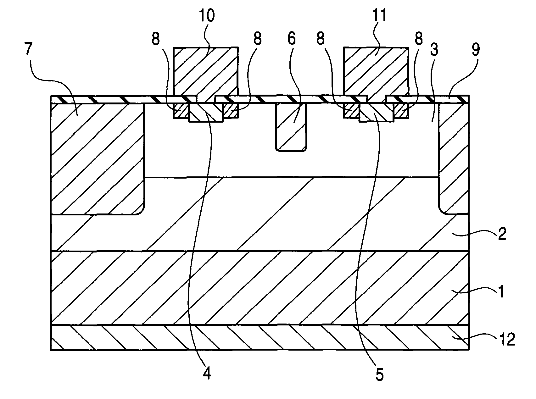
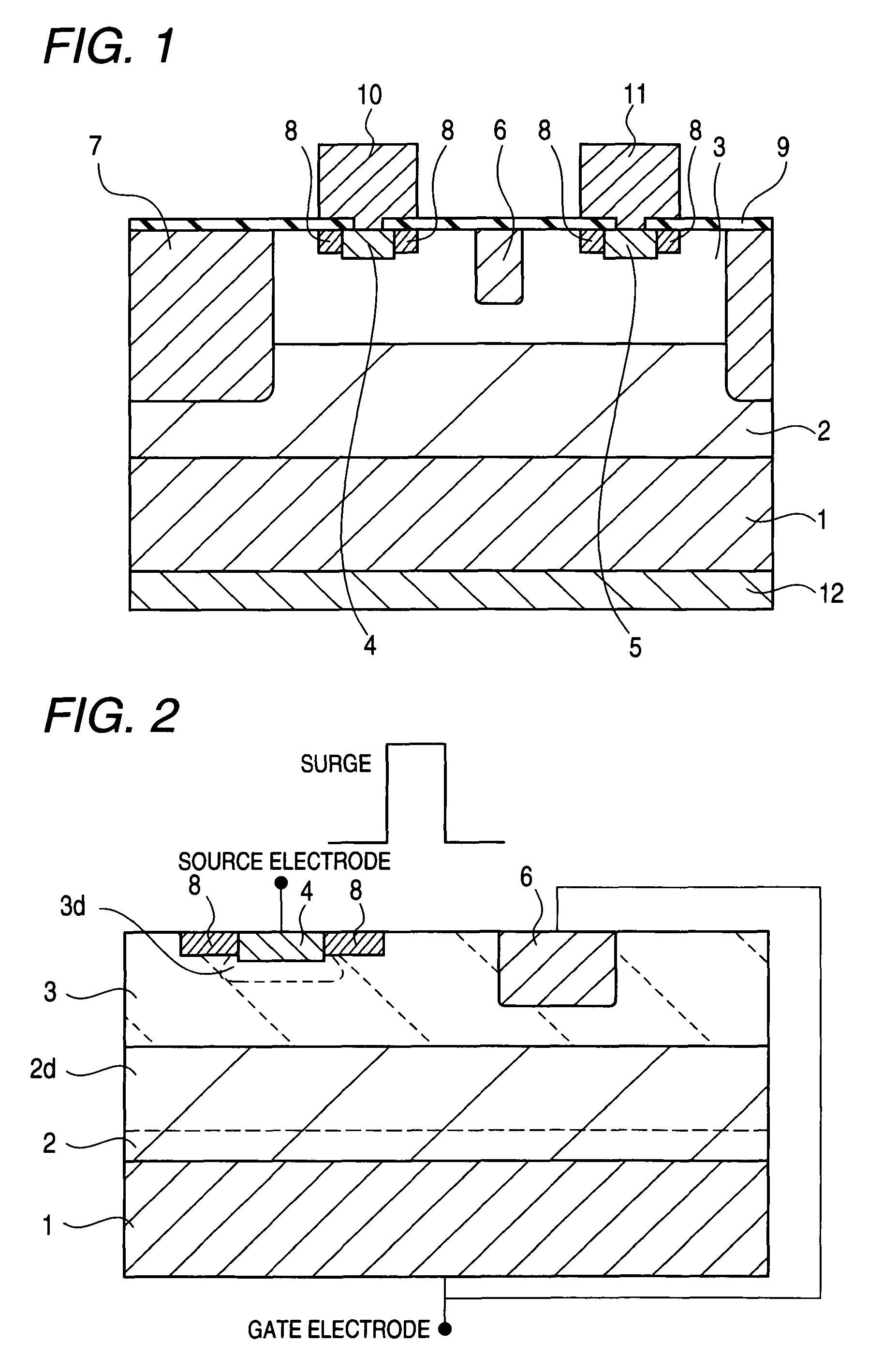
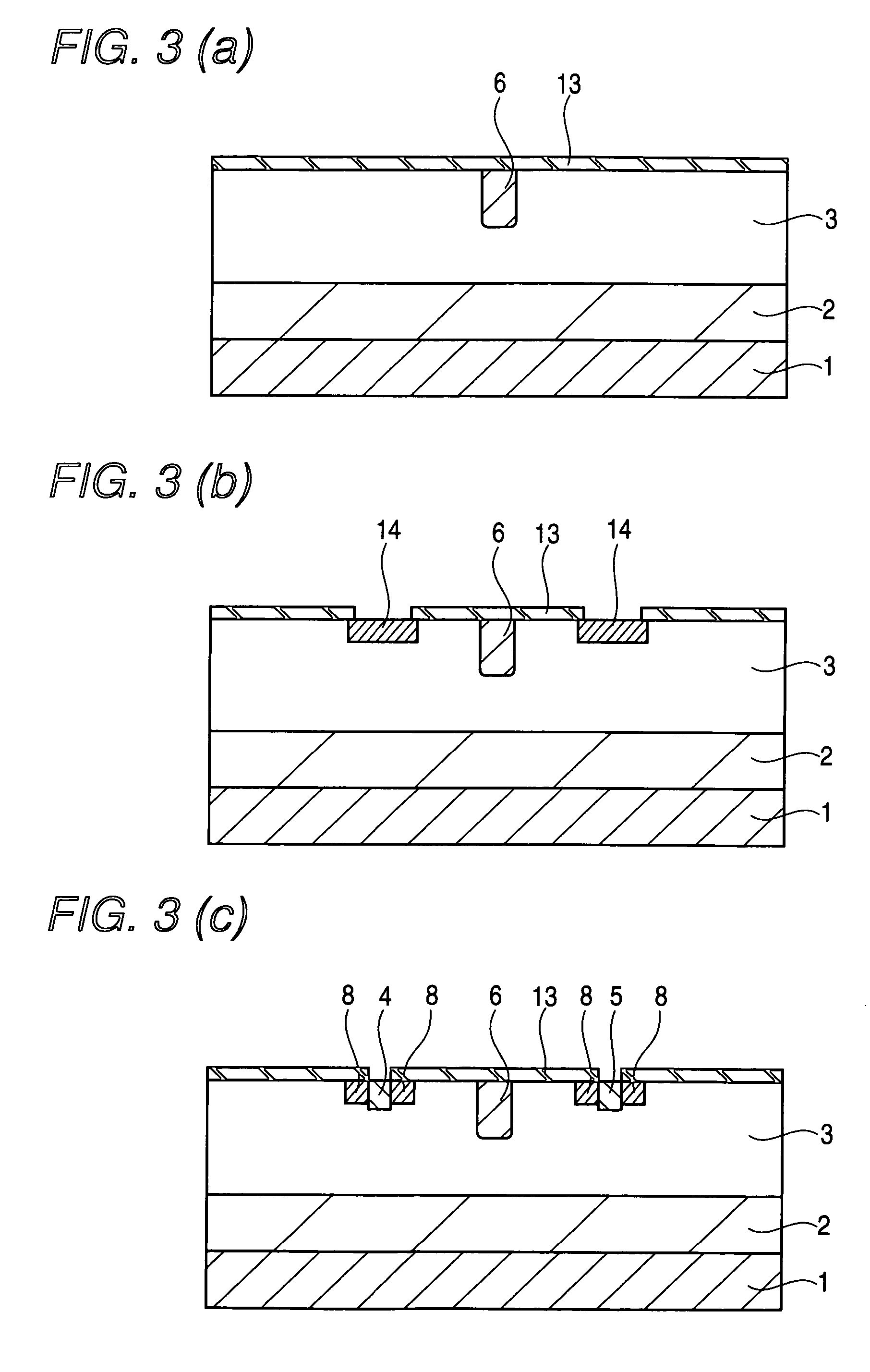
[0040]FIG. 1 is a cross-sectional view showing the basic structure of J-FET of the first embodiment of the invention. In the drawing, the same parts as those described in the section of the related art are designated by the same reference numerals as therein. This embodiment is characterized in that a short-circuit preventing layer 8 that comprises a diffusion layer of a reverse conduction type is formed around a source diffusion layer 4 and a drain diffusion layer 5 to be in contact with the side walls thereof. In FIG. 1, a P-type epitaxial layer 2 having an impurity concentration of 1×1015 cm−3 and a thickness of 10 μm is formed on a P++-conductive substrate 1 having an impurity concentration of 1020 cm−3 or so; and an N-type epitaxial layer 3 having an impurity concentration of 5×1015 cm−3 and a thickness of 5 μm is formed thereon. The P-type epitaxial layer 2 is formed for relaxing the auto-doping from the P++-conductive substrate 1.

[0041]In the N-type epitaxial ...

second embodiment

of the Invention

[0057]FIG. 8 is a cross-sectional view showing the basic structure of J-FET of the second embodiment of the invention. Different from the structure of the first embodiment mentioned above, this structure is characterized in that the short-circuit preventing layer 8 is provided between the source diffusion layer 4 or the drain diffusion layer 5 and the gate diffusion layer 6, spaced a little from the source diffusion layer 4 or the drain diffusion layer 5 not in contact with it.

[0058]This embodiment is described briefly hereinunder with reference to FIG. 8. The same parts as those described in the first embodiment are designated by the same reference numerals as therein. In FIG. 8, a P-type epitaxial layer 2 and an N-type epitaxial layer 3 are formed on a P++-conductive substrate 1. In the N-type epitaxial layer 3, formed are N+-conductive source diffusion layer 4 and drain diffusion layer 5, and P+-conductive gate diffusion layer 6. As in FIG. 8, a short-circuit prev...

third embodiment

of the Invention

[0061]FIG. 9 is a cross-sectional view showing the basic structure of J-FET of the third embodiment of the invention. Different from the structures of the first and second embodiments mentioned above, this structure is characterized in that a short-circuit preventing layer 8n is formed in contact with the side walls of the source diffusion layer 4 or the drain diffusion layer 5, and it is a diffusion layer of the same conduction type as that of the source diffusion layer 4 and the drain diffusion layer 5.

[0062]This embodiment is described briefly hereinunder with reference to FIG. 9. The same parts as those described in the first embodiment are designated by the same reference numerals as therein. In FIG. 9, a P-type epitaxial layer 2 and an N-type epitaxial layer 3 are formed on a P++-conductive substrate 1. In the N-type epitaxial layer 3, formed are N+-conductive source diffusion layer 4 and drain diffusion layer 5, and a P+-conductive gate diffusion layer 6. As i...


PUM


Abstract

To improve the surge resistance of J-FET, a P-type epitaxial layer 2 and an N-type epitaxial layer 3 are formed on a P++-conductive substrate 1; N+-conductive source diffusion layer 4 and drain diffusion layer 5, and a p+-conductive gate diffusion layer 6 are formed in the N-type epitaxial layer 3; and a short-circuit preventing layer 8 of a reversed conduction-type diffusion layer is formed adjacent to the side walls of the source diffusion layer 4 and the drain diffusion layer 5. Having the constitution, the punch-through to be caused by surge voltage is prevented in the surface region of the device, and the surge resistance thereof is improved. Via the holes formed in a protective insulation film 9 on the surface of the device, a source electrode 10 connected to the source diffusion layer 4, and a drain electrode 11 connected to the drain diffusion layer 5 are formed on the surface side of the device. A gate electrode 12 is formed on the back of the substrate 1, and this is connected to the gate diffusion layer 6 via a contact diffusion layer 7 formed in the device.

Description

BACKGROUND OF THE INVENTION[0001]1. Field of the Invention[0002]The present invention relates to a semiconductor device and a method for producing it, and in particular to the improvement in the surge resistance of a semiconductor device having a junction field-effect transistor (hereinafter abbreviated to J-FET).[0003]2. Description of the Related Art[0004]A conventional J-FET has a basic structure that comprises a P-type epitaxial layer 2 formed on a P++-conductive substrate 1; an N-type epitaxial layer 3 on the P-type epitaxial layer 2; and an N+-conductive source diffusion layer 4, an N+-conductive drain diffusion layer 5 and a P+-conductive gate diffusion layer 6 formed in the N-type epitaxial layer 3, as in FIG. 15. A P+-conductive contact diffusion layer 7 is formed, and this is connected to the gate diffusion layer 6 at a site not shown in the drawing A source electrode 10 and a drain electrode 11 are formed, and they are connected to the source diffusion layer 4 and the dra...

Claims


Application Information

Patent Timeline
Patent Type & Authority Patents(United States)
IPC IPC(8): H01L29/74H01L21/335H01L29/812H01L21/337H01L21/338H01L29/10H01L29/772H01L29/808
CPCH01L29/1095H01L29/66901H01L29/808
Inventor GUNJI, HIROYUKIOTAKI, TETSUSHI
Owner PANASONIC SEMICON SOLUTIONS CO LTD
Why Eureka
Try Eureka