Metal foil interconnection of electrical devices

a technology of metal foil and electrical devices, which is applied in the direction of electrical apparatus construction details, semiconductor/solid-state device details, and support structure mounting, etc., can solve the problems of poor ic reliability, ic failure and even explosive failure of the ic, interconnection failure, and increase the cost, volume and weight of the ic, so as to reduce the resistance increase the reliability of the interconnecting elemen

Active Publication Date: 2011-08-30
RAYTHEON CO
View PDF6 Cites 2 Cited by
  • Summary
  • Abstract
  • Description
  • Claims
  • Application Information

AI Technical Summary

Benefits of technology

[0013]It is an object of the present invention to provide an electrical interconnecting element suitable for interconnecting a power IC with a substrate module and interconnecting between power ICs with reduced inductance in the interconnecting elements.
[0014]It is an object of the present invention to provide an electrical interconnecting element suitable for interconnecting a power IC with a substrate module and interconnecting between power ICs with reduced resistance in the interconnecting elements.
[0015]It is an object of the present invention to provide an electrical interconnecting element suitable for interconnecting a power IC with a substrate module and interconnecting between power ICs with increased reliability of the interconnecting elements.
[0018]A method for electrically interconnecting an electrical device (112, 412) to a substrate module (114, 214) includes solder bonding or otherwise attaching the bottom surface of the electrical device (112, 412) and specifically the third conductive device surface (C) to the third conductive substrate surface (C1). Further electrical interconnection of electrical device (112, 412) to the substrate module (114, 214) includes bonding or otherwise electrically interconnecting a first conductive foil element (302, 402) to each of a plurality of discrete conductive first device surfaces (A) positioned on the electrical device (112, 412) to electrically interconnect the discrete device surfaces (A) to each other. The method includes bonding or otherwise electrically interconnecting the first conductive foil element (302, 402) to one or two first conductive substrate surfaces (A1 and A2) positioned on the substrate module (114, 414). This electrically interconnects each of the discrete device surfaces (A) to one or two of the substrate module surfaces (A1 and A2). The first conductive foil element (302, 402) also can serve as an interconnect from substrate surface A1 to substrate surface A2, thus eliminating the need for such an interconnection on the substrate. This reduces the routing area required on the substrate, reduces current loop areas, and the associated parasitics.
[0022]Other metals can be placed where required to bond to other surfaces, e.g. gold plated to permit bonding to gold surfaces. It should be noted that in areas away from the bonding areas, thicker metal can be used to reduce interconnection parasitics. It is advantageous and efficient to be able to mass produce a single interconnection assembly that is comprised of a dielectric film and the required interconnection metal pieces. This single piece is easier to handle and bond in place as compared to freestanding individual pieces. The single interconnection piece can be formed to unique three dimensional shapes to follow the topology required to provide interconnection to devices and substrates that may be at different heights. Both the metal structures and the dielectric layers can be formed using mechanical methods such as thermoforming. Bonding the dielectric material prior to performing the metal to metal interconnection bonding may be useful to ensure the flexible foil assembly does not move during the metal bonding operations.
[0026]A method for electrically interconnecting an electrical device (412) to a substrate module (214) includes attaching the bottom surface of the electrical device (412) to the substrate conductive surface (C1). Further electrical interconnection of electrical device (412) to the substrate module (214) includes bonding or otherwise electrically interconnecting the first conductive foil element (402) to each of a plurality of discrete first conductive device surfaces (A) positioned on the electrical device (412). This electrically interconnects the discrete device surfaces (A) to each other. The method includes bonding or otherwise electrically interconnecting the first conductive foil element (402) to one or two conductive first substrate surfaces (A1 and A2) positioned on the substrate module (214). This electrically interconnects each of the discrete device surfaces (A) to the substrate module surfaces (A1 and or A2). The first conductive foil element (402) also can serve as an interconnect from substrate surface A1 to substrate surface A2, thus eliminating the need for such an interconnection on the substrate. This reduces the routing area required on the substrate, reduces current loop areas, and the associated parasitics. Foil element (402) also serves to provide off module interconnection.

Problems solved by technology

Undesirable parasitics, such as, parasitic inductance and parasitic resistance, associated with wire bond interconnection, can induce large voltage and current spikes in the IC leading to poor IC reliability, IC failure and even explosive failure of the IC.
To compensate for interconnection parasitics, it has been necessary to over-design power IC circuits with increased design margins and this has lead to reduce power efficiencies and increases in the cost, volume and weight of the ICs.
Another problem caused by the rapid on-off current flow over conventional interconnecting wire bonds is that the bond wires are susceptible to rapidly varying electro-thermal-mechanical stress which can lead to interconnection failures.
In particular, rapid changes in current flow produce rapid heating and therefore rapid thermal expansion and contraction of the larger diameter relatively stiff wire material.
This action can lead to fatigue failure at the wire bond contact points which will lead to increased current and therefore stress on remaining bond connections, thereby reducing the reliability of the overall electrical system.

Method used


Image

  • Metal foil interconnection of electrical devices
  • Metal foil interconnection of electrical devices
  • Metal foil interconnection of electrical devices

Examples


Embodiment Construction

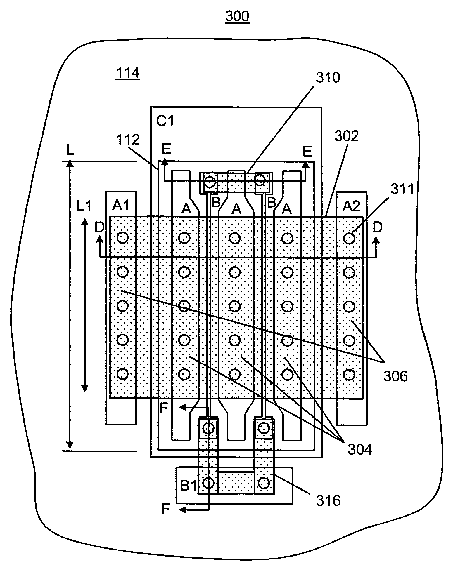
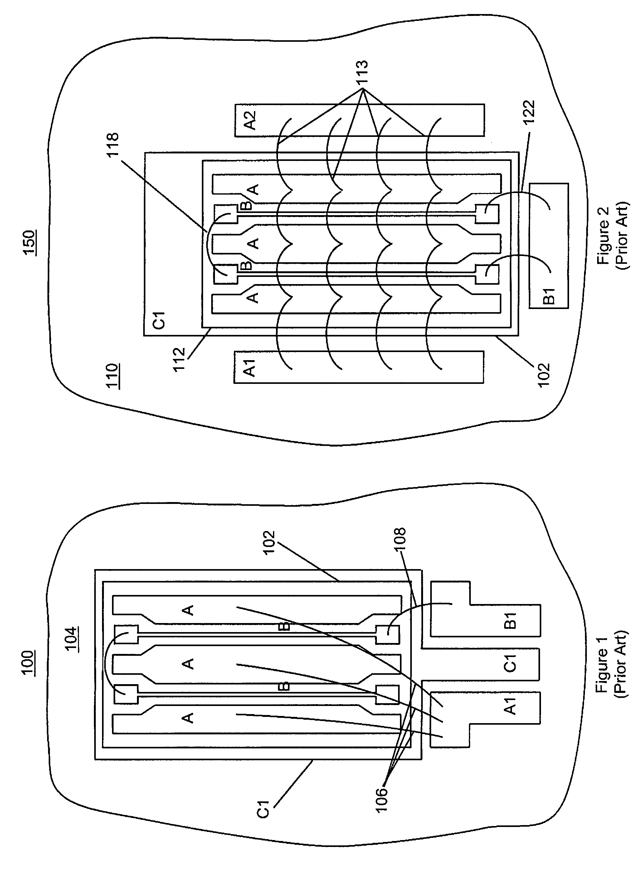
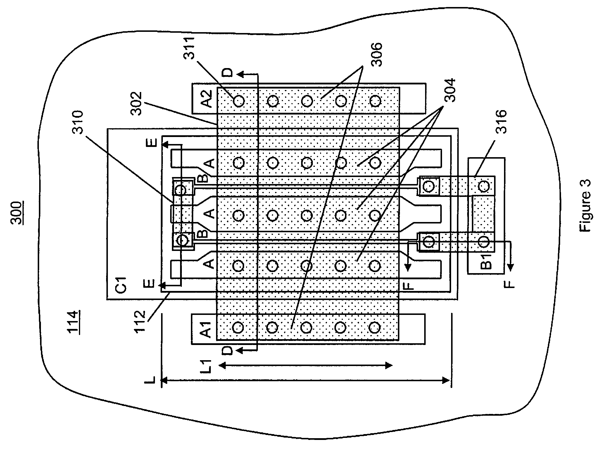
[0040]Referring to FIG. 1 a schematic representation of a first embodiment 100 of a conventional unpackaged electronic device 102 e.g. an integrated circuit (IC) or chip, supported on a substrate module 104 is shown in top view. An outer package or housing, not shown, supports and protects the electronic device 102 and substrate module 104 against moisture and contaminates as well as provides an electromagnetic shield.

[0041]The electronic device 102 includes a plurality of conductive device surfaces A and B, disposed on a top surface of the device 102 and a conductive device surface C, not shown, on the bottom surface of the device 102. Alternately, or additionally, other conductive device surfaces may be disposed on other surfaces of the packaged electronic device 102. Each conductive device surface A, B, and C comprises a conductive metal, e.g. aluminum, or a conductive bondable material, or the like suitable for collecting surface charges thereon and or conducting current thereth...


PUM

PropertyMeasurementUnit
diametersaaaaaaaaaa
thicknessaaaaaaaaaa
thickaaaaaaaaaa

Abstract

An electrical assembly (300, 400) includes a power IC such as a MOSFET (112, 412) attached to a substrate module (114, 214). The MOSFET includes a top surface comprising first and second conductive device surfaces (A, B), associated with first and second device ports, and a bottom surface comprising a third conductive device surface C associated with a third device port. A first foil element is bonded to the first conductive device surface(s) A and to each of the first conductive substrate surfaces (A1, A2) and provides a continuous conductive pathway from each conductive surface (A) to each other conductive surface (A) and to each conductive surface (A1, A2). A second foil element is bonded to the second conductive device surface(s) B and to the second conductive substrate surface B1 and provides a continuous conductive pathway from each device conductive surface (B) to the substrate conductive surface (B1). A third foil element may be installed to electrically interconnect the discrete second device surfaces (B). The foil elements reduce interconnection parasitics and reduce charge and thermal energy density at device conductive surfaces as compared to wire bonded electrical interconnections. The foil elements may be comprised of formed metal elements that are flexible but sufficiently rigid to hold a formed shape or flexible foils supported on a flexible dielectric substrate.

Description

BACKGROUND OF THE INVENTION[0001]1. Field of the Invention[0002]The present invention relates to an improved method and apparatus for making electrical interconnects between power semiconductor devices and a substrate module and specifically to interconnecting power semiconductor devices with a substrate module using a formed conductive foil element or a formed flexible interconnection assembly comprised of a supporting dielectric film and conductive foil elements.[0003]2. Description of the Related Art[0004]Power semiconductor devices, or power integrated circuits (ICs), used as switches or rectifiers in power electronic circuits, and the like, often operate at considerably higher power and current density levels than other semiconductor devices.[0005]Generally power ICs are enclosed or packaged in a housing formed with exposed conductive surfaces serving as IC input / output terminals or gates. Typically the packaged IC is positioned on a substrate module such as a lead frame or on ...

Claims


Application Information

Patent Timeline
Patent Type & Authority Patents(United States)
IPC IPC(8): H05K1/11
CPCH01L23/49844H01L24/36H01L24/40H01L24/49H01L24/84H01L24/45H01L2224/45014H01L2224/45015H01L2224/45124H01L2224/48091H01L2224/4813H01L2224/48132H01L2224/48227H01L2224/4911H01L2224/49113H01L2224/49171H01L2224/49175H01L2224/83205H01L2224/85424H01L2224/85455H01L2924/01005H01L2924/01013H01L2924/01027H01L2924/01028H01L2924/01029H01L2924/01074H01L2924/01078H01L2924/01079H01L2924/01082H01L2924/13055H01L2924/13091H01L2924/14H01L2924/2076H01L2924/30107H01L2924/3025H01L24/48H01L2924/01006H01L2924/01033H01L2924/014H01L2224/37124H01L2224/37147H01L2924/1306H01L2924/1301H01L2924/1305Y10T29/49165Y10T29/4913Y10T29/49144Y10T29/49158H01L2924/00014H01L2924/00H01L2924/351H01L2224/45147H01L2224/48824H01L2224/48855H01L2224/48724H01L2224/48755H01L2224/40095H01L2224/84205H01L2224/40225H01L24/37H01L2224/83801H01L2924/20755H01L2924/00015H01L2924/2075H01L2924/20754H01L2924/206H01L2224/73221
Inventor GUINN, KEITH V.
Owner RAYTHEON CO
Why Eureka
Try Eureka