
Semiconductor LED, opto-electronic integrated circuits (OEIC), and method of fabricating OEIC

a technology of optoelectronic integrated circuit and semiconductor, which is applied in the direction of semiconductor devices, solid-state devices, optical waveguide light guides, etc., can solve the problem that no silicon light emitting diode has been obtained, and achieves high luminescence efficiency and high efficiency

Inactive Publication Date: 2011-10-04
HITACHI LTD
View PDF3 Cites 17 Cited by
  • Summary
  • Abstract
  • Description
  • Claims
  • Application Information

AI Technical Summary

Benefits of technology

The present invention provides a light emitting diode (LED) made of silicon or germanium, which can be efficiently fabricated on a silicon substrate using existing silicon processes. The LED has a high luminescence efficiency and includes a thin layer of single crystalline silicon that acts as a waveguide for guiding light. The invention also provides a device based on a Group IV semiconductor that can perform laser oscillation using a waveguide laser cavity. The invention solves the problem of obtaining a silicon LED and allows for the development of more efficient and effective optical communication devices.

Problems solved by technology

Unfortunately, no one succeeded in obtaining a silicon light emitting diode until now, and a structure for building a light emitting diode within one chip and causing light emission was something no one could imagine.

Method used


Image

  • Semiconductor LED, opto-electronic integrated circuits (OEIC), and method of fabricating OEIC
  • Semiconductor LED, opto-electronic integrated circuits (OEIC), and method of fabricating OEIC
  • Semiconductor LED, opto-electronic integrated circuits (OEIC), and method of fabricating OEIC

Examples


embodiment 1

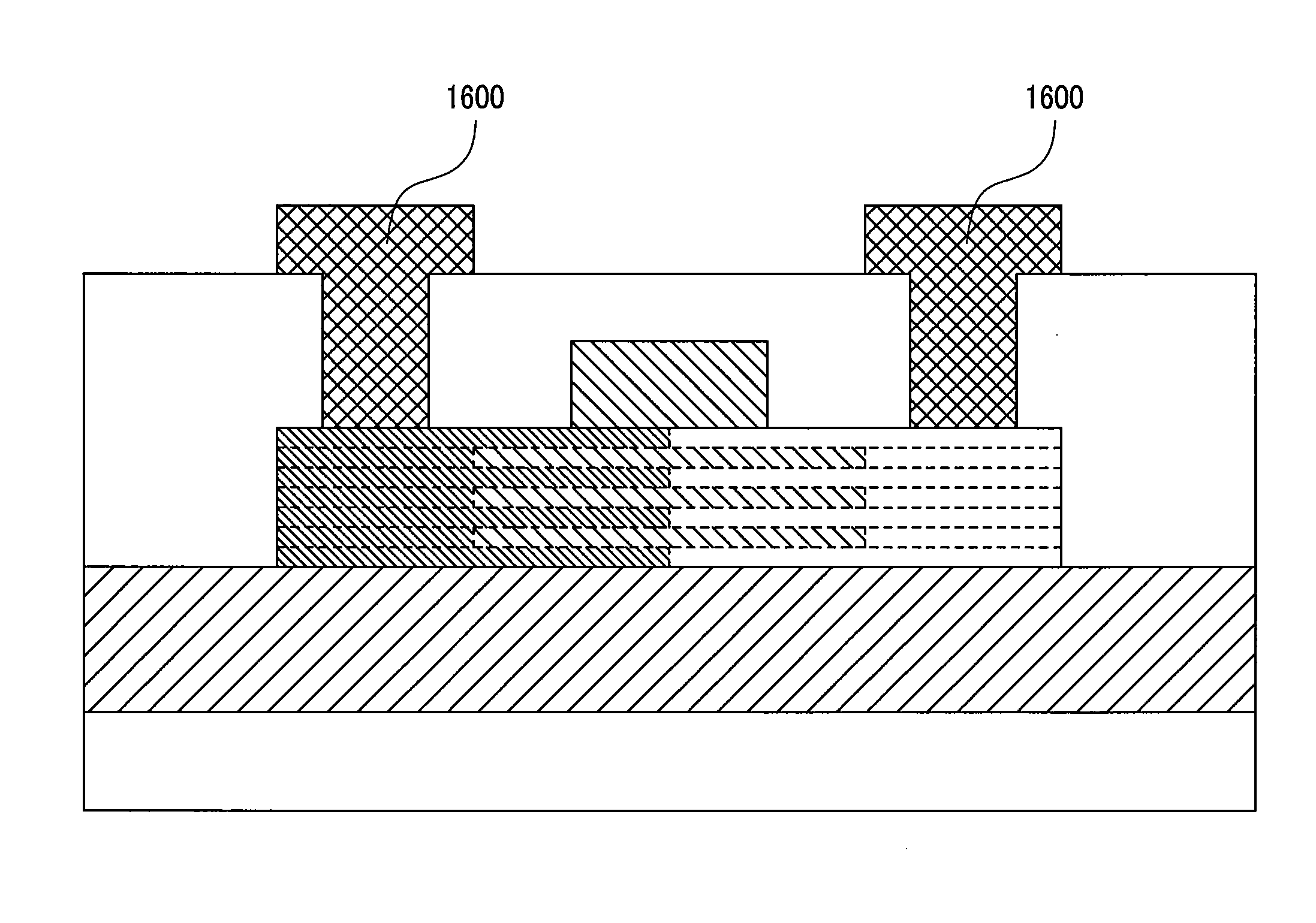
[0134]FIG. 11 is a planar layout for an integrated light emitting diode according to the present invention; FIG. 12 is a planar layout for a light receiving element according to the present invention; and FIGS. 13 through 18 are schematic cross-sectional views for stepwisely explaining the fabricating process of the integrated light emitting diode. In each of the drawings, a cross-sectional view taken along line A-A′ of the planar layout (FIG. 11) is shown on the left hand side, and a cross-sectional view taken along line B-B′ of the planar layout (FIG. 11) is shown on the right hand side.

[0135]A 1 μm thick silicon oxide film 1900 is formed on a silicon support substrate 1100 and an SOI wafer having a 100 nm thick single crystalline silicon layer 1120 is thermally oxidized on the silicon oxide film, to form a 20 nm oxide film (FIG. 13). A silicon thin film formation region (fin) and a contact region are formed (FIG. 14) by using an active region pattern 1150 shown in FIG. 11. Herein...

embodiment 2

[0149]In this embodiment, a plurality of fins are employed as an integrated light emitting diode. The fins can be formed, independently of the patterning. A so-called spacer process is employed as follows. FIG. 43 shows an exemplary planar layout, and FIGS. 45 through 60 stepwisely show the fabricating process by using cross-sectional views (A-A′ cross section of FIG. 43). This method is based on a dummy pattern 1152, but the dummy pattern can be arranged in two different forms, i.e., a convex pattern or a hole pattern. FIG. 43 shows a convex pattern, and FIG. 44 shows a hole pattern. According to the fabricating process of this embodiment, after the dummy pattern 1152 of FIG. 43 and FIG. 44 is formed, fins are self-aligned with respect to the dummy pattern. In general, because of the self-alignment, spacers 1202, 1203, 1204, 1205, 1981, 1982, and 1983 used for fin formation are not necessarily found in a photo mask, but they are indicated at pattern positions of the layout after th...

embodiment 3

[0177]This embodiment discloses a luminous region expansion method that does not require a laminate film or plural wall-type silicon thin films disclosed in Embodiment 1 and Embodiment 2. In a light emitting diode according to this embodiment, as shown in FIG. 69, silicon semiconductor regions 3303 and 3304 of different conductive types are arranged adjacent each other on a silicon oxide film 3302 formed on the surface of the silicon substrate 3301, and a silicon oxide film 3305 is formed in the periphery of the interface of these two semiconductor regions only in such a manner that it covers a portion of the surfaces of the two semiconductor regions. Meanwhile, a silicide 3306, the compound of silicon and a metal, is formed on the surface of a semiconductor region that is not covered with the silicon oxide film 3305. In addition, a part of the silicon substrate 3301, that is, the silicon substrate in a region having the light emitting diode formed thereon, is removed to expose the ...


PUM


Abstract

A light emitting diode demonstrating high luminescence efficiency and comprising a Group IV semiconductor such as silicon or germanium equivalent thereto as a basic component formed on a silicon substrate by a prior art silicon process, and a fabricating method of waveguide thereof are provided. The light emitting diode of the invention comprises a first electrode for implanting electrons, a second electrode for implanting holes, and a light emitting section electrically connected to the first and the second electrode, wherein the light emitting section is made out of single crystalline silicon and has a first surface and a second surface facing the first surface, wherein with respect to plane orientation (100) of the first and second surfaces, the light emitting section crossing at right angles to the first and second surfaces is made thinner, and wherein a material having a high refractive index is arranged around the thin film section.

Description

CLAIM OF PRIORITY[0001]The present application claims priority from Japanese application JP2007-036328, filed on Feb. 16, 2007, the content of which is hereby incorporated by reference into this application.BACKGROUND OF THE INVENTION[0002]1. Field of the Invention[0003]The present invention relates to a semiconductor light emitting diode (LED), an opto-electronic integrated circuit (OEIC), and a method of fabricating the OEIC; and, more particularly, to an integrated semiconductor, which is in a mixed arrangement with a semiconductor integrated circuit performing an electric signal processing and which integrates a high-brightness LED, a phototransistor capable of controlling optical output power / wavelength with a gate voltage, a silicon laser element, a light receiving element, and a waveguide, and methods of fabricating them.[0004]2. Description of the Related Arts[0005]Optical communications are used in broadband networks supporting the Internet industry. Optical transmission an...

Claims


Application Information

Patent Timeline
Patent Type & Authority Patents(United States)
IPC IPC(8): H01L27/15H01L33/34H01L33/44H01L33/16
CPCG02B6/13H01L27/15H01L33/34G02B6/43H01L33/02H01S5/32
Inventor HISAMOTO, DIGHSAITO, SHINICHIKIMURA, SHINICHIRO
Owner HITACHI LTD
Learn More