Heating apparatus, heat treatment apparatus, computer program and storage medium

a heat treatment apparatus and heat treatment technology, applied in the field of heat treatment apparatus, heat treatment apparatus, computer program and storage medium, can solve the problems of reducing heating efficiency, significantly longer life, and reducing heat capacity of heating lamps, so as to achieve rapid heating and cooling, the effect of effective solving the problem

Active Publication Date: 2011-10-18
TOKYO ELECTRON LTD
View PDF31 Cites 424 Cited by
  • Summary
  • Abstract
  • Description
  • Claims
  • Application Information

AI Technical Summary

Benefits of technology

[0029]The present invention has been conceived in view of the problems mentioned above to effectively solve the problems. Therefore, the purpose of the present invention is to provide a heating apparatus capable of optimizing a wavelength of heating light emitted from an LED element and thus rapidly heating up and cooling down only a shallow surface portion of a target object such as a semiconductor wafer or the like, while maintaining a uniform temperature distribution regardless of the kinds of films. The present invention further provides a heat treatment apparatus using same, a computer program and a storage medium.
[0031]Due to applying a plurality of heating light sources each including an LED element that emits heating light with a wavelength of 360 to 520 nm toward a target object, the wavelength of the heating light is optimized. As a result, it is possible to rapidly heat up and cool down only a surface of the object such as a semiconductor wafer or the like, with a reduced thickness and under a uniform temperature distribution state regardless of the kinds of films.
[0050]It is preferable that the control unit is capable of controlling electric current directions and electric powers of the thermoelectric conversion devices independently and, when heating the object, the control unit controls the heat treatment apparatus in such a way that the thermoelectric conversion devices are independently heated or cooled to thereby increase in-plane temperature uniformity of the object.
[0056]The heating apparatus, the heat treatment apparatus using the same, the computer program and the storage medium in accordance with the present invention are capable of accomplishing superior operational effects as follows.
[0057]Due to applying a plurality of heating light sources each including an LED element that emits heating light with a wavelength of 360 to 520 nm toward a target object, the wavelength of the heating light is optimized. As a result, it is possible to rapidly heat up and cool down only a surface of the object such as a semiconductor wafer or the like, with a reduced thickness and under a uniform temperature distribution state regardless of the kinds of films.

Problems solved by technology

However, as the semiconductor devices become highly dense, multilayered and highly integrated, heat treatment methods grow more and more stringent year by year.
The LED element or the laser generates far less heat in itself than does a heating lamp and has a significantly longer life and a lower heat capacity than those of the heating lamp.
This poses a problem in that, despite an intention to heat only a shallow portion under a wafer surface, the heating light reaches a deep position of the wafer and heats up a deep portion thereof, consequently allowing impurities to be diffused into the deep portion under the wafer surface.
Furthermore, since the light emitted from the halogen lamp has the long wavelength as noted above and unnecessarily heats up the deep portion under the wafer surface, heating efficiency is reduced and thus it is necessary to use high output power, thereby causing reduction in energy efficiency.
Therefore, just like the halogen lamp set forth above, there is a problem in that the flash lamp heats up a deep portion of a wafer.
As a consequence, there is a problem in that a temperature difference which may cause lateral stresses in minute regions is generated or a wafer is locally melted, depending on the kinds of films or the wavelength of the light.
This entails a problem in that the structure thereof becomes complicated.
However, the mere use of the LED element does not guarantee optimization of the wavelength of the emitted light and, therefore, it is difficult to selectively and uniformly heat only the surface portion of a wafer in such a way that the depth of impurity diffusion regions is kept small and the concentration of impurities is kept high enough to meet the recent design rule requirement.

Method used


Image

  • Heating apparatus, heat treatment apparatus, computer program and storage medium
  • Heating apparatus, heat treatment apparatus, computer program and storage medium
  • Heating apparatus, heat treatment apparatus, computer program and storage medium

Examples


Embodiment Construction

[0072]Hereinafter, one embodiment of a heating apparatus, a heat treatment apparatus and a storage medium in accordance with the present invention will be described in detail with reference to the accompanying drawings.

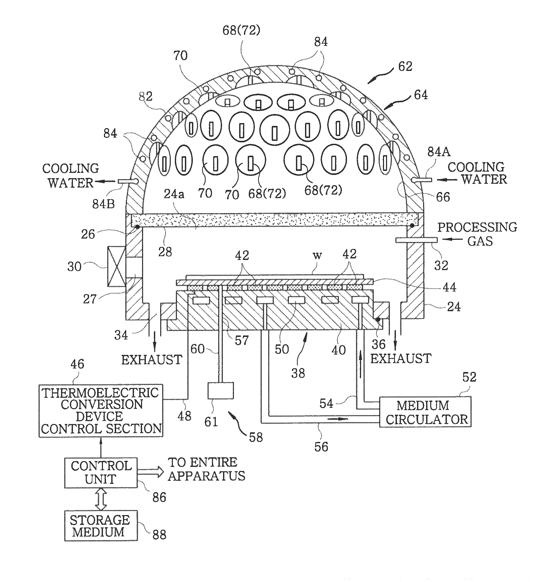
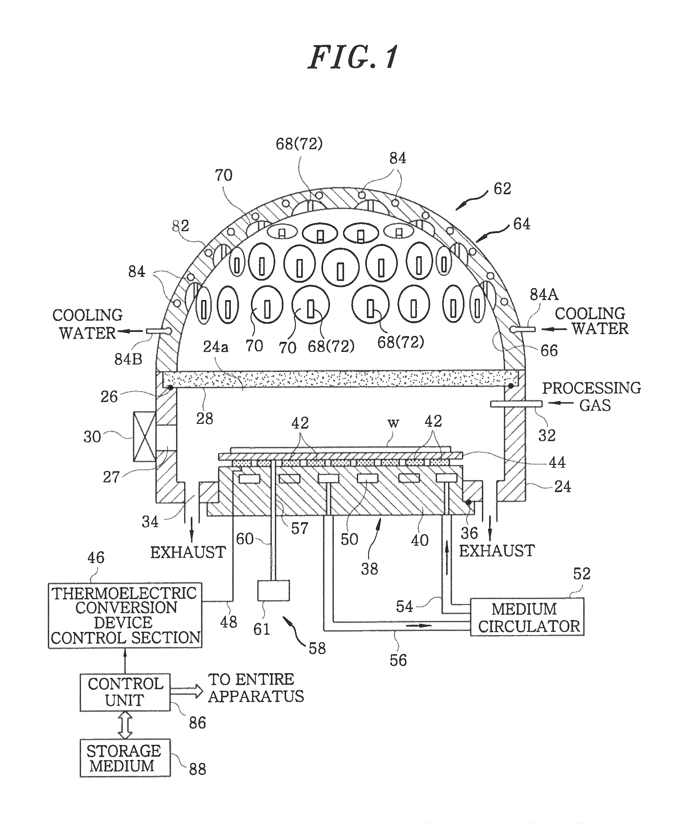
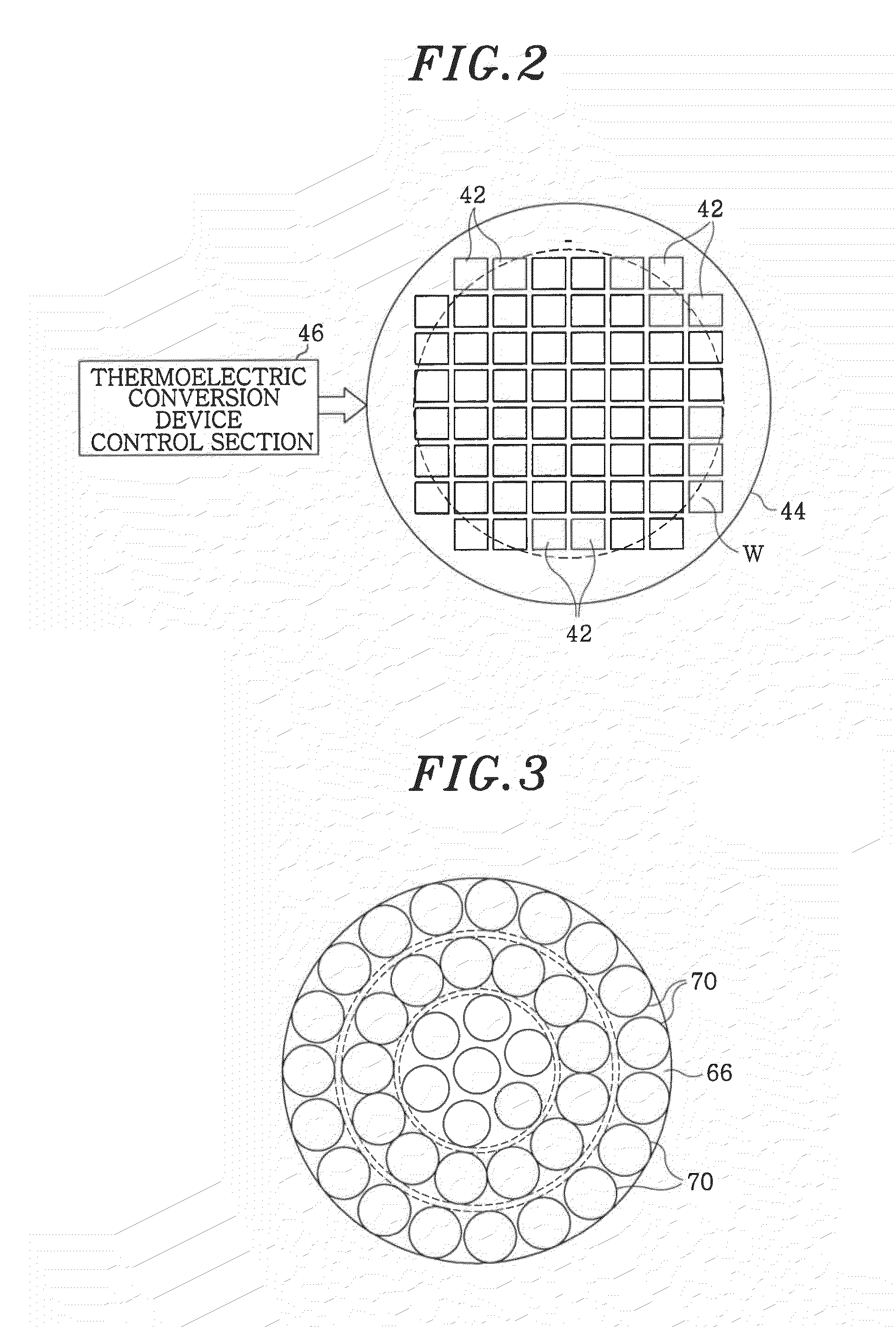
[0073]FIG. 1 is a cross sectional configuration view showing one example of a heat treatment apparatus in accordance with the present invention; FIG. 2 is a plan view illustrating an arrangement state of thermoelectric conversion devices; FIG. 3 is a view illustrating an arrangement of reflectors when a heating apparatus is viewed from a table; FIG. 4 is a view illustrating a path of heating light emitted from semiconductor light emitting devices of a heating light source; FIG. 5 is an enlarged cross sectional view showing an element attachment rod to which the semiconductor light emitting devices are attached; and FIG. 6 is an enlarged perspective view showing a tip end portion of the element attachment rod.

[0074]Referring to FIG. 1, a heat treatment apparatus 22 inc...


PUM

PropertyMeasurementUnit
wavelengthaaaaaaaaaa
central wavelengthaaaaaaaaaa
wavelengthaaaaaaaaaa

Abstract

A heating apparatus for heating a target object W is provided with a plurality of heating light sources, including LED elements for applying heating light having a wavelength within a range from 360 to 520 nm to the object. Thus, a temperature of only the shallow surface of the object, such as a semiconductor wafer, is increased / reduced at a high speed in uniform temperature distribution, irrespective of the film type.

Description

[0001]This application is a Continuation Application of PCT International Application No. PCT / JP2006 / 321764 filed on Oct. 31, 2006, which designated the United States.FIELD OF THE INVENTION[0002]The present invention relates to a heating apparatus for irradiating heating light on a semiconductor wafer or the like, a single-wafer heat treatment apparatus for performing a specified heat treatment to a semiconductor wafer or the like through the use of the heating apparatus, a computer program and a storage medium.BACKGROUND OF THE INVENTION[0003]In the manufacture of semiconductor devices, it is typical that various kinds of heat treatments, such as film forming, pattern etching, oxidation / diffusion, reforming and annealing, are repeatedly performed to a semiconductor wafer to thereby manufacture desired devices. However, as the semiconductor devices become highly dense, multilayered and highly integrated, heat treatment methods grow more and more stringent year by year. In particular...

Claims


Application Information

Patent Timeline
Patent Type & Authority Patents(United States)
IPC IPC(8): F26B19/00
CPCH01L21/2686H01L21/324H01L21/67115H01L21/26H01L21/265
Inventor KASAI, SHIGERUSUZUKI, TOMOHIRO
Owner TOKYO ELECTRON LTD
Why Eureka
Try Eureka