Light-emitting device

a technology of light-emitting devices and scan lines, which is applied in the direction of instruments, static indicating devices, etc., can solve the problems of large consumption current, difficult to and excessive loading of output portions so as to reduce the potential of signal lines, prevent excessive loading, and ensure the reliability of scan line driver circuits

Inactive Publication Date: 2011-10-25
SEMICON ENERGY LAB CO LTD
View PDF25 Cites 7 Cited by
  • Summary
  • Abstract
  • Description
  • Claims
  • Application Information

AI Technical Summary

Benefits of technology

[0005]General light-emitting devices include a transistor (a driving transistor) for controlling current supplied to a light-emitting element in each pixel. In order to supply current which is necessary for light emission to the light-emitting element, it is necessary to ensure a big potential difference between a pixel electrode and a common electrode of the light-emitting element. In addition, since a potential applied to the pixel electrode is applied from a power supply line through the driving transistor, amplitude which is large enough to control a potential difference between the pixel electrode and the common electrode normally is needed as the amplitude of a signal for controlling a gate of the driving transistor. In conventional light-emitting devices, this amplitude is supplied by signals from signal lines, and the amount of consumption current is large due to charging and discharging of the signal lines. However, in the light-emitting device disclosed in Reference 1, a potential applied to a gate of a driving transistor is controlled with a signal line when a potential difference is generated between a pixel electrode and a common electrode; and the potential applied to the gate of the driving transistor is controlled with a scan line when a potential difference is not generated between the pixel electrode and the common electrode. That is, a path for controlling the potential when the driving transistor is turned on and a path for controlling the potential when the driving transistor is turned off are varied from each other. Therefore, it is acceptable as long as signals input to the signal lines can control either the potential for turning on the driving transistor or the potential for turning off the driving transistor, so that the amplitude of the signals can be decreased. In other words, since the amplitude of the potentials of the signal lines that are frequently charged with electricity and discharged in a pixel portion can be decreased, power consumption of the signal line driver circuit can be reduced; consequently, power consumption of the whole light-emitting device can be reduced.
[0007]In view of the foregoing problems, the amplitude of a potential of a signal line is decreased and a scan line driver circuit is prevented from being excessively loaded.
[0011]In the present invention, as the path for applying a potential to the gate electrode of the driving transistor, paths are provided separately from a scan line and a signal line. Thus, the amplitude of a potential of the signal line can be decreased and a scan line driver circuit can be prevented from being excessively loaded. Accordingly, even if a pixel portion has a larger screen or higher definition, the reliability of the scan line driver circuit can be ensured; consequently, the reliability of the light-emitting device can be ensured. Further, power consumption of the whole light-emitting device can be reduced.

Problems solved by technology

In conventional light-emitting devices, this amplitude is supplied by signals from signal lines, and the amount of consumption current is large due to charging and discharging of the signal lines.
Thus, when the number of pixels which share one scan line is increased as the pixel portion has higher definition or when the length and resistance of the scan lines are increased as the screen becomes larger, the output portion of the scan line driver circuit is excessively loaded.
Accordingly, there is a problem in that it is difficult to ensure the reliability of the scan line driver circuit or that it is difficult to operate the scan line driver circuit.
In particular, such a problem is remarkable in a light-emitting device whose display portion exceeds 10 inches.

Method used


Image

  • Light-emitting device
  • Light-emitting device
  • Light-emitting device

Examples


embodiment mode 1

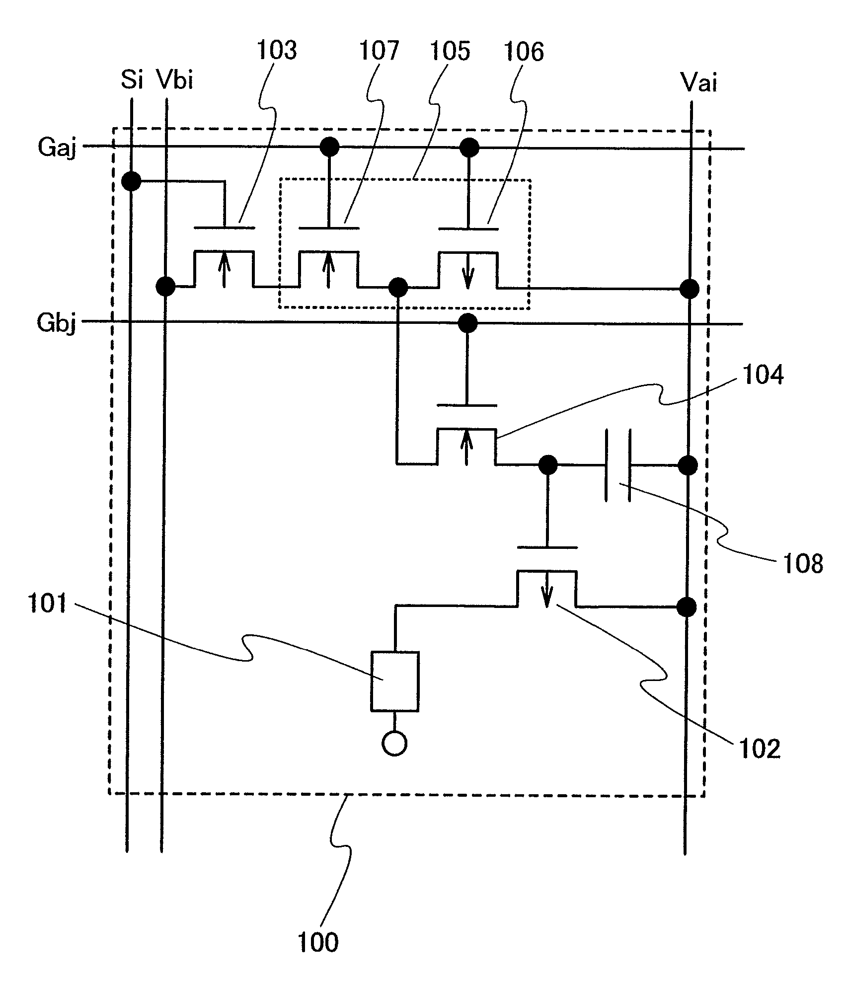
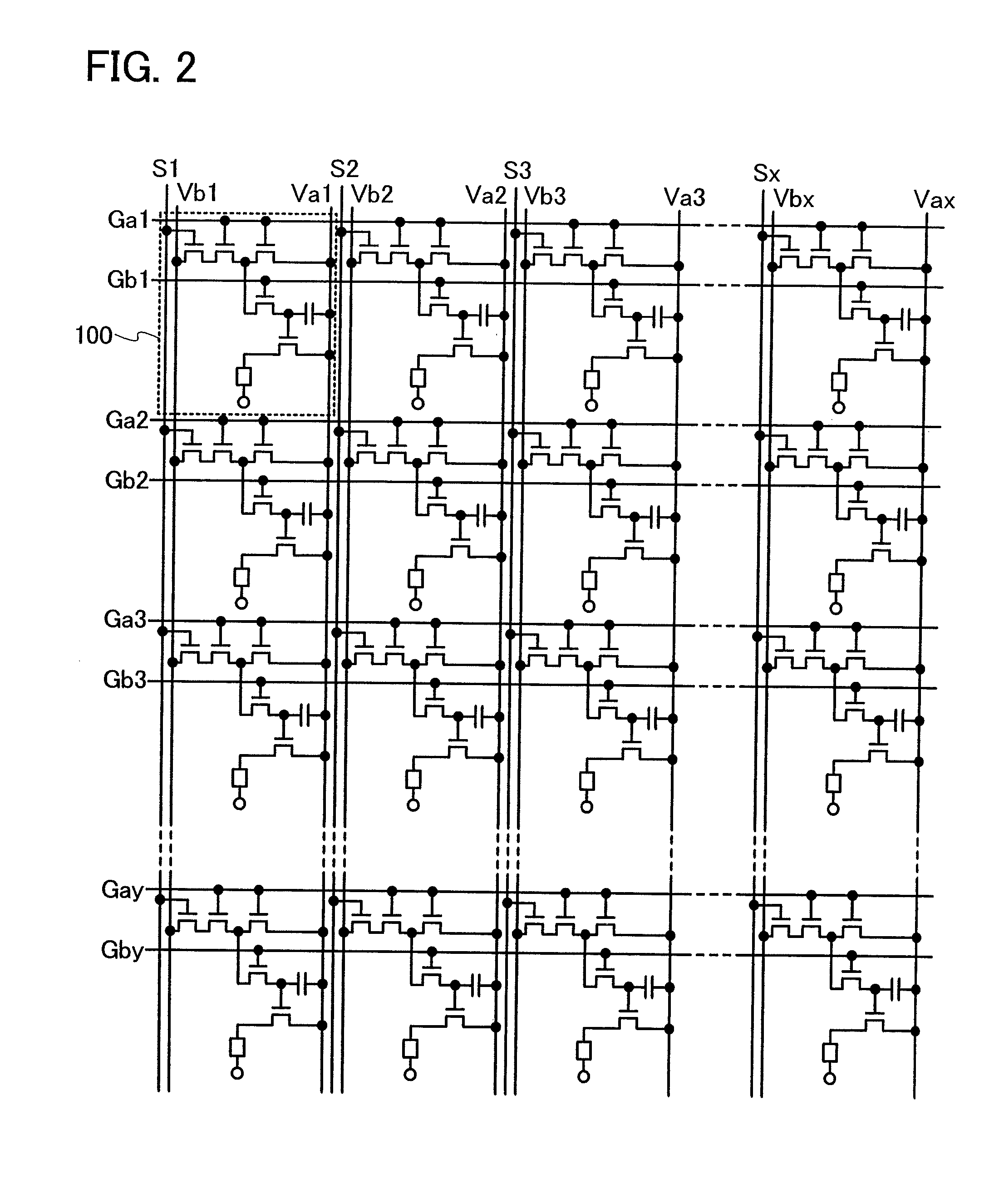
[0033]In this embodiment mode, the structure of a pixel included in a light-emitting device that is one mode illustrated in this specification is described. FIG. 1 shows a circuit diagram of a pixel included in the light-emitting device that is one mode illustrated in this specification as an example. A pixel 100 shown in FIG. 1 includes at least a light-emitting element 101, a first power supply line Vai (i is any one of 1 to x) having a first potential, a second power supply line Vbi (i is any one of 1 to x) having a second potential, a first transistor 102, a second transistor 103, a third transistor 104, and a switch 105.

[0034]The light-emitting element 101 includes a pixel electrode, a common electrode, and an electroluminescent layer to which current is supplied through the pixel electrode and the common electrode. A connection between the first power supply line Vai and the pixel electrode of the light-emitting element 101 is controlled by the first transistor 102. Note that ...

embodiment mode 2

[0072]Next, a method for manufacturing a light-emitting device that is one mode illustrated in this specification is described in detail. Note that although a thin film transistor (TFT) is shown as an example of a semiconductor element in this embodiment mode, a semiconductor element used for the light-emitting device that is one mode illustrated in this specification is not limited to this. For example, a memory element, a diode, a resistor, a capacitor, an inductor, or the like can be used instead of a TFT.

[0073]First, as shown in FIG. 9A, an insulating film 401 and a semiconductor film 402 are sequentially formed over a substrate 400 having heat resistance. It is possible to form the insulating film 401 and the semiconductor film 402 successively.

[0074]A glass substrate such as a barium borosilicate glass substrate or an aluminoborosilicate glass substrate, a quartz substrate, a ceramic substrate, or the like can be used as the substrate 400. Alternatively, a metal substrate such...

embodiment 1

[0158]In this embodiment, a method for manufacturing a light-emitting device that is one mode illustrated in this specification, by which a semiconductor element is formed by using a semiconductor film which is transferred from a semiconductor substrate (a bond substrate) to a support substrate (a base substrate), is described.

[0159]First, as shown in FIG. 16A, an insulating film 901 is formed over a bond substrate 900. The insulating film 901 is formed using an insulating material such as silicon oxide, silicon oxynitride, silicon nitride oxide, or silicon nitride. The insulating film 901 can be formed using either a single insulating film or by stacking a plurality of insulating films. For example, in this embodiment, the insulating film 901 is formed by stacking silicon oxynitride containing more oxygen than nitrogen and silicon nitride oxide containing more nitrogen than oxygen in that order from the bond substrate 900 side.

[0160]For example, in the case of using silicon oxide f...


PUM


Abstract

The amplitude of a potential of a signal line is decreased and a scan line driver circuit is prevented from being excessively loaded. A light-emitting device includes a light-emitting element; a first power supply line having a first potential; a second power supply line having a second potential; a first transistor for controlling a connection between the first power supply line and the light-emitting element; a second transistor, which is controlled in accordance with a video signal, whether outputting the second potential applied from the second power supply line or not; a switching element for selecting either the first potential applied from the first power supply line or the output of the second transistor; and a third transistor for selecting whether the first potential or the output of the second transistor which is selected by the switch is applied to a gate of the first transistor.

Description

TECHNICAL FIELD[0001]The present invention relates to a light-emitting device using a light-emitting element.BACKGROUND ART[0002]Since light-emitting devices using light-emitting elements have high visibility, are suitable for reduction in thickness, and do not have limitations on viewing angle, they have attracted attention as display devices which are alternatives to CRTs (cathode ray tube) or liquid crystal display devices. There are a scan line driver circuit and a signal line driver circuit as typical examples of a driver circuit included in an active matrix light-emitting device. A plurality of pixels are selected every one line or every plurality of lines by a scan line driver circuit. Then, video signals are input to the pixels included in the selected line by a signal line driver circuit through a signal line.[0003]In recent years, the number of pixels in an active matrix light-emitting device has been increased in order to display images with higher definition and higher r...

Claims


Application Information

Patent Timeline
Patent Type & Authority Patents(United States)
IPC IPC(8): G09G3/10
CPCG09G3/3225G09G2300/043G09G2330/025G09G2320/0223G09G2300/0866G09G3/30G09G3/32G09G3/3233
Inventor FUKUMOTO, RYOTAMIYAKE, HIROYUKITANADA, YOSHIFUMITAKAHASHI, KEI
Owner SEMICON ENERGY LAB CO LTD
Why Eureka
Try Eureka