Diffusion barrier layers

a diffusion barrier and layer technology, applied in the direction of vacuum evaporation coating, semiconductor/solid-state device details, coatings, etc., can solve the problems of affecting the performance of the device, excessive capacitance, and affecting the dielectric properties of the devi

Inactive Publication Date: 2011-11-08
NOVELLUS SYSTEMS
View PDF49 Cites 12 Cited by
  • Summary
  • Abstract
  • Description
  • Claims
  • Application Information

AI Technical Summary

Benefits of technology

[0023]The combined seed and diffusion barrier layer may be a part of the overall integrated circuit metallization layer that also includes dielectric and circuit lines. The combined layer is positioned between and in contact with the dielectric and the circuit line. The layer prevents migration of conductive line materials, such as copper, into the dielectric. The layer may include one or more elements selected from groups IVB, VB, and VIB in the periodic table. More specifically, the layer may include tantalum, titanium, zirconium, and / or hafnium. To prevent oxidation of the layer when exposed to ambient conditions, the layer may also include a passivation layer of sulfides, selenides, and / or tellurides of the materials forming the layer. In certain embodiments, the thickness of the combined layer may be no greater than about 15 nm. Thinner layers are particularly beneficial for use with narrower conductive lines.

Problems solved by technology

Some conductive metals, for example copper, can diffuse into the dielectric material that forms the trench or provides a surface and can impact dielectric properties.
Maintaining low dielectric constants (low-k) is particularly important in ICs having densely packed features, where the insulating dielectric is thin and can lead to excessive capacitance.
This can cause signal delay (RC time constant) and crosstalk between conducting lines, thus adversely affecting the performance of the device.
Many barrier materials are poor electronic conductors in comparison to copper and aluminum and also are resistive to initiating uniform and adherent electroplating thereupon.
However, each such layer adds to production costs and complicates reducing the size of device nodes.
Further miniaturization of IC devices results in constantly decreasing dimensions of device features.
Electroplating copper or other material into such small features can present a set of challenges.
However, reducing thicknesses of these layers may lead to undesirable results.
Moreover, many diffusion barrier materials do not adhere well to underlining dielectrics leading to poor Time Dependent Dielectric Breakdown (TDDB) behavior and Electromigration (EM) performance, both of which can cause premature failure of the IC, particularly in smaller circuit lines.

Method used


Image

  • Diffusion barrier layers
  • Diffusion barrier layers
  • Diffusion barrier layers

Examples


Embodiment Construction

[0038]In the following description, numerous details are set forth in order to provide a thorough understanding of the present invention. The present invention may be practiced without some or all of these details. In other instances, well known process operations have not been described in detail to not unnecessarily obscure the present invention. While the invention will be described in conjunction with the specific embodiments, it will be understood that it is not intended to limit the invention to the embodiments. References herein to physical vapor deposition, chemical vapor deposition, and atomic layer deposition are intended to cover many variants of these processes, including processes that are assisted with plasma, vacuum or low pressure processes, atmospheric pressure processes, etc.

Introduction

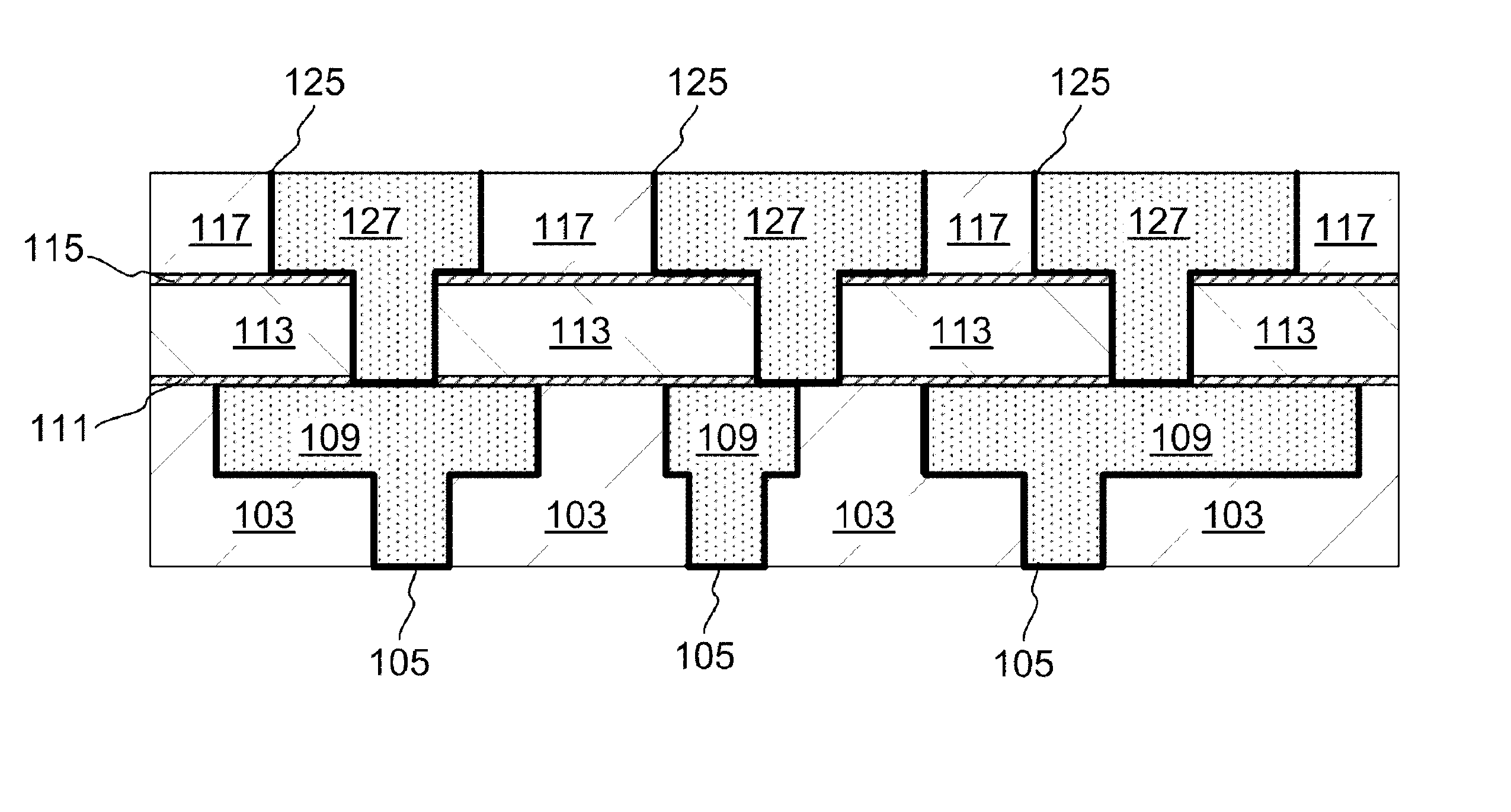
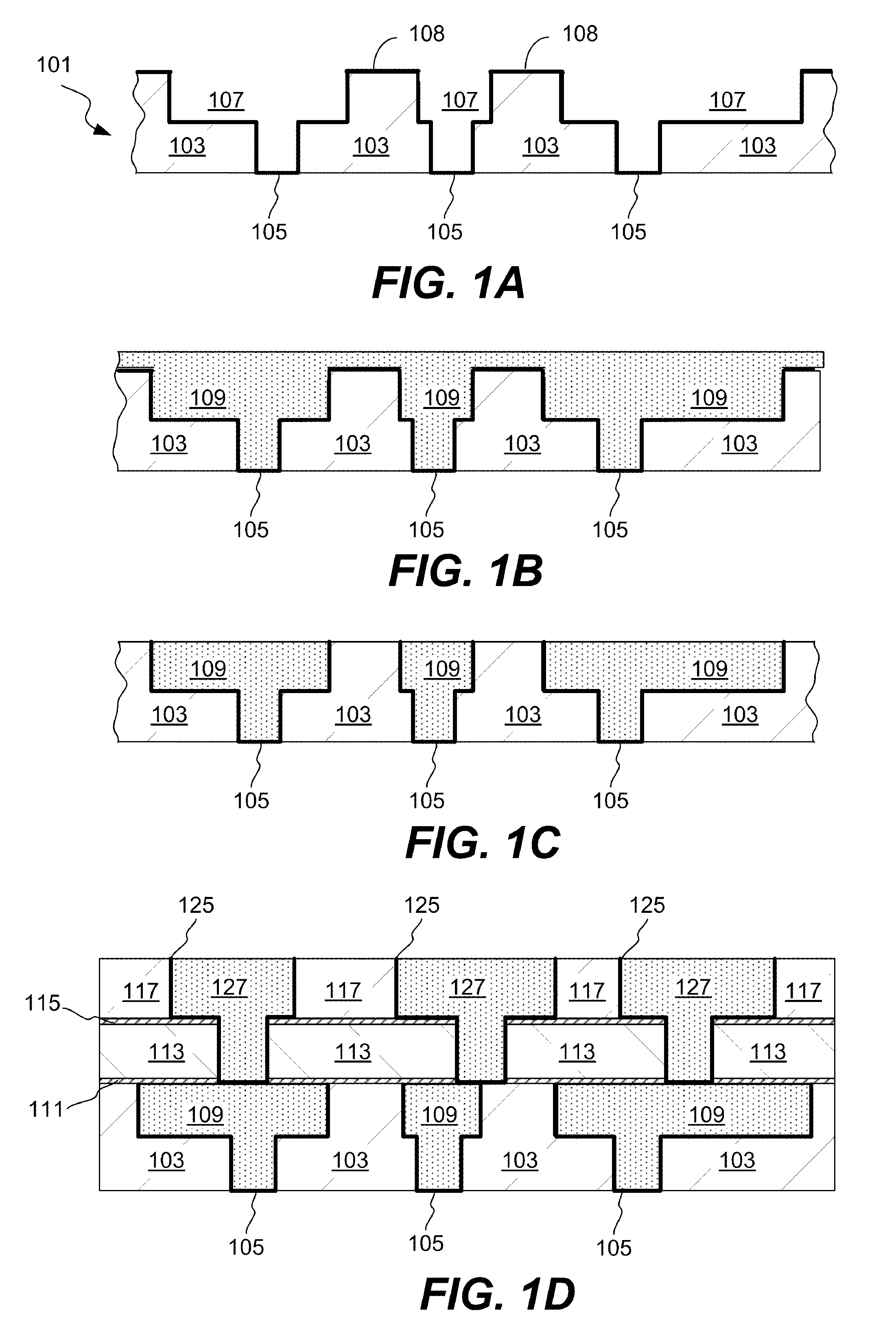
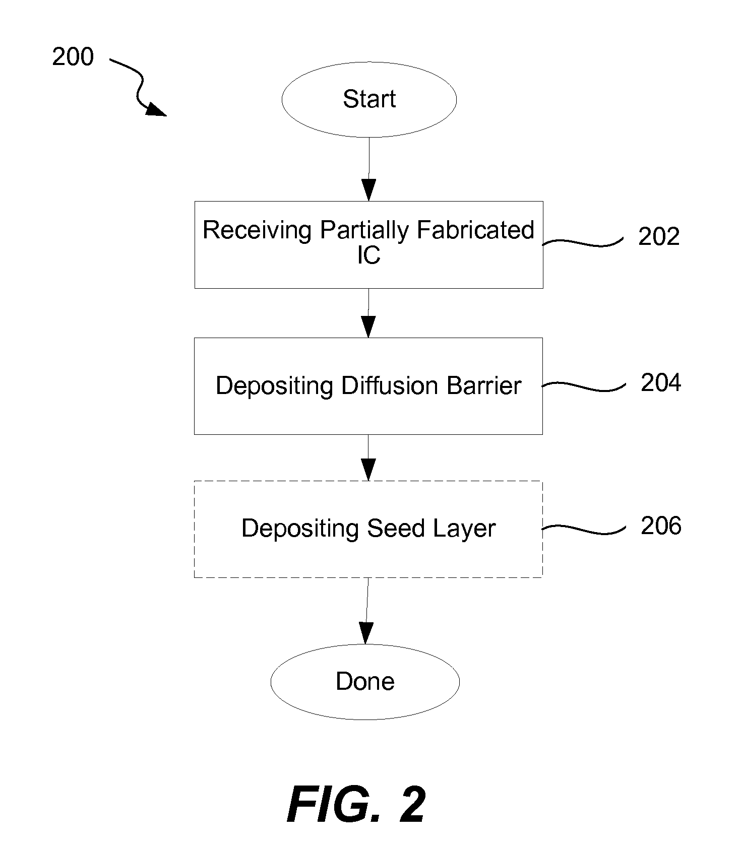
[0039]Improved methods and apparatuses for deposition and further processing of diffusion barriers are disclosed herein. Integrated circuit (IC) metallization layers including diffu...


PUM

PropertyMeasurementUnit
thicknessaaaaaaaaaa
sheet resistanceaaaaaaaaaa
widthaaaaaaaaaa

Abstract

Provided are methods and apparatuses for depositing barrier layers for blocking diffusion of conductive materials from conductive lines into dielectric materials in integrated circuits. The barrier layer may contain copper. In some embodiments, the layers have conductivity sufficient for direct electroplating of conductive materials without needing intermediate seed layers. Such barrier layers may be used with circuits lines that are less than 65 nm wide and, in certain embodiments, less than 40 nm wide. The barrier layer may be passivated to form easily removable layers including sulfides, selenides, and / or tellurides of the materials in the layer.

Description

FIELD OF THE INVENTION[0001]The present invention relates generally to methods and an apparatus for fabricating integrated circuits and more particularly to methods and an apparatus for depositing a diffusion barrier for blocking diffusion of conductive metals from circuit lines into dielectric materials in integrated circuits.BACKGROUND OF THE INVENTION[0002]Integrated circuit (IC) fabrication methods generally involve deposition of conductive metals into recessed features and other surfaces forming a layer of inter-layer dielectric (ILD). The deposited metal provides the conductive paths, which extend horizontally and vertically within the IC substrate, connecting the active devices (e.g., transistors) in a desired pattern. The metal lines formed in adjacent ILD layers are connected to each other by a series of interconnections (interconnects). On a typical wafer substrate, one or several dielectric layers are deposited onto a layer containing the active devices and are patterned ...

Claims


Application Information

Patent Timeline
Patent Type & Authority Patents(United States)
IPC IPC(8): H01L21/70
CPCC23C14/06C23C14/0623C23C14/3414H01L21/2855H01L21/28556H01L21/28562H01L21/76843H01L21/76846H01L21/76856H01L21/76858H01L21/76864H01L21/76873H01L21/76898H01L23/53238H01L23/53295H01L2924/0002H01L2924/00
Inventor MOUNTSIER, THOMAS W.SHAVIV, ROEYMAYER, STEVEN T.POWELL, RONALD A.
Owner NOVELLUS SYSTEMS
Why Eureka
Try Eureka