Plasma display panel and method for producing the same

Inactive Publication Date: 2011-11-22
PANASONIC CORP
View PDF10 Cites 0 Cited by
  • Summary
  • Abstract
  • Description
  • Claims
  • Application Information

AI Technical Summary

Benefits of technology

[0033]In accordance with the method of the present invention, the glass component comprises an alkyl group, and thus it is made possible to decrease the difference in thermal expansion between “dielectric layer” and “glass substrate/display electrodes” upon the heating of the dielectric material. As a result, the occurrence of the cracking phenomenon attributable to the difference in thermal expansion can be effectively prevented or reduced. In use of the PDP, the second dielectric layer can prevent the gas originating in the residual alkyl group from being released to an internal space of the PDP, which makes it possible to avoid such a trouble from occurring as the released gas is adsorbed to the phosphor layer of the rear panel, thus deteriorating the phosphor layer. As a result, there is realized a plasma display panel with a higher efficiency of light emission and a lesser deterioration of brightness.
[0034]In the PDP obtained by the producin

Problems solved by technology

However, a size reduction of the discharge cells leads to a decrease in emission brightness and thus an increase in power consumption.
However, even in this method, the emission brightness is still insufficient and a further improvement is required.
Although the dielectric constant can be decreased by adding other substances (e.g. alkali metal), a highly conductive metal such as silver is used as a main component in an electrode of PDP, and thus a diffusion and colloidization of the silver are promoted due to ion migration, which leads to an yellowing phenomenon in the dielectric body.
Although these processes can produce a dielectric layer with a high purity and a low dielectric constant, expensive vacuum facilities are required and a film-for

Method used


Image

  • Plasma display panel and method for producing the same
  • Plasma display panel and method for producing the same
  • Plasma display panel and method for producing the same

Examples


examples

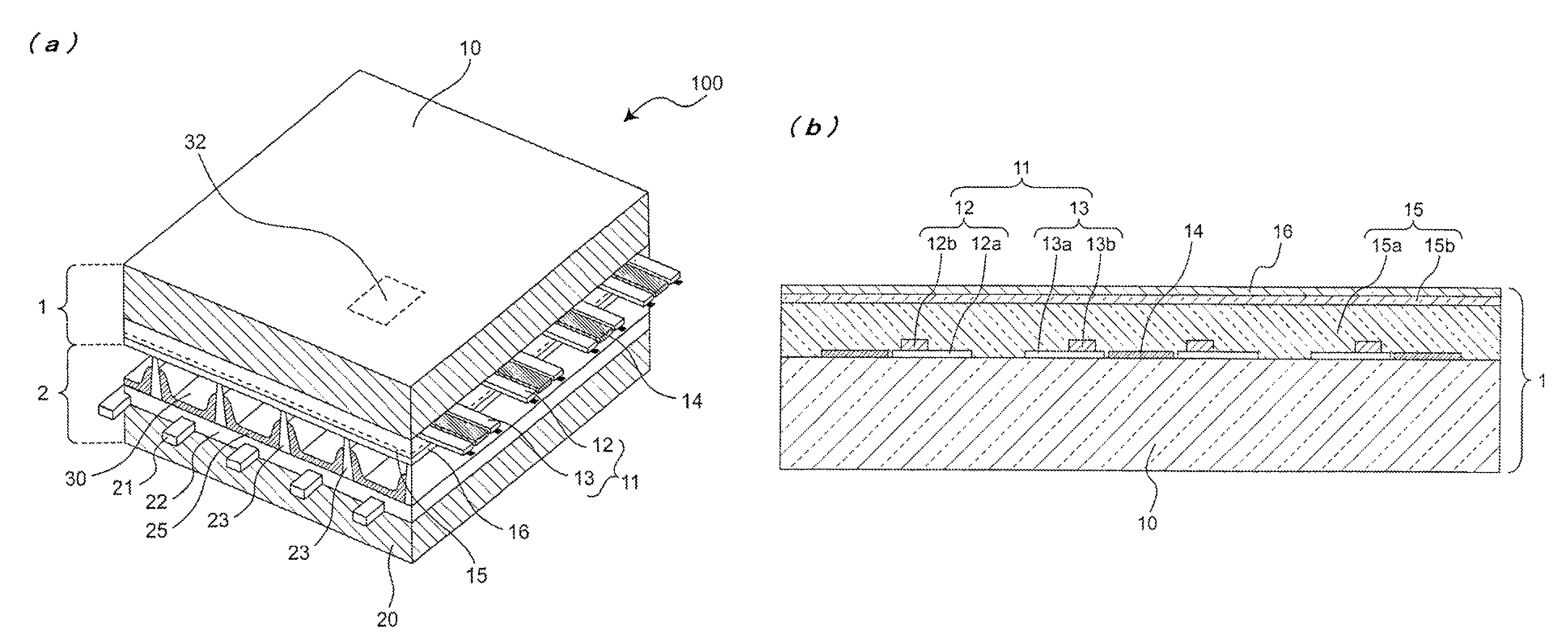
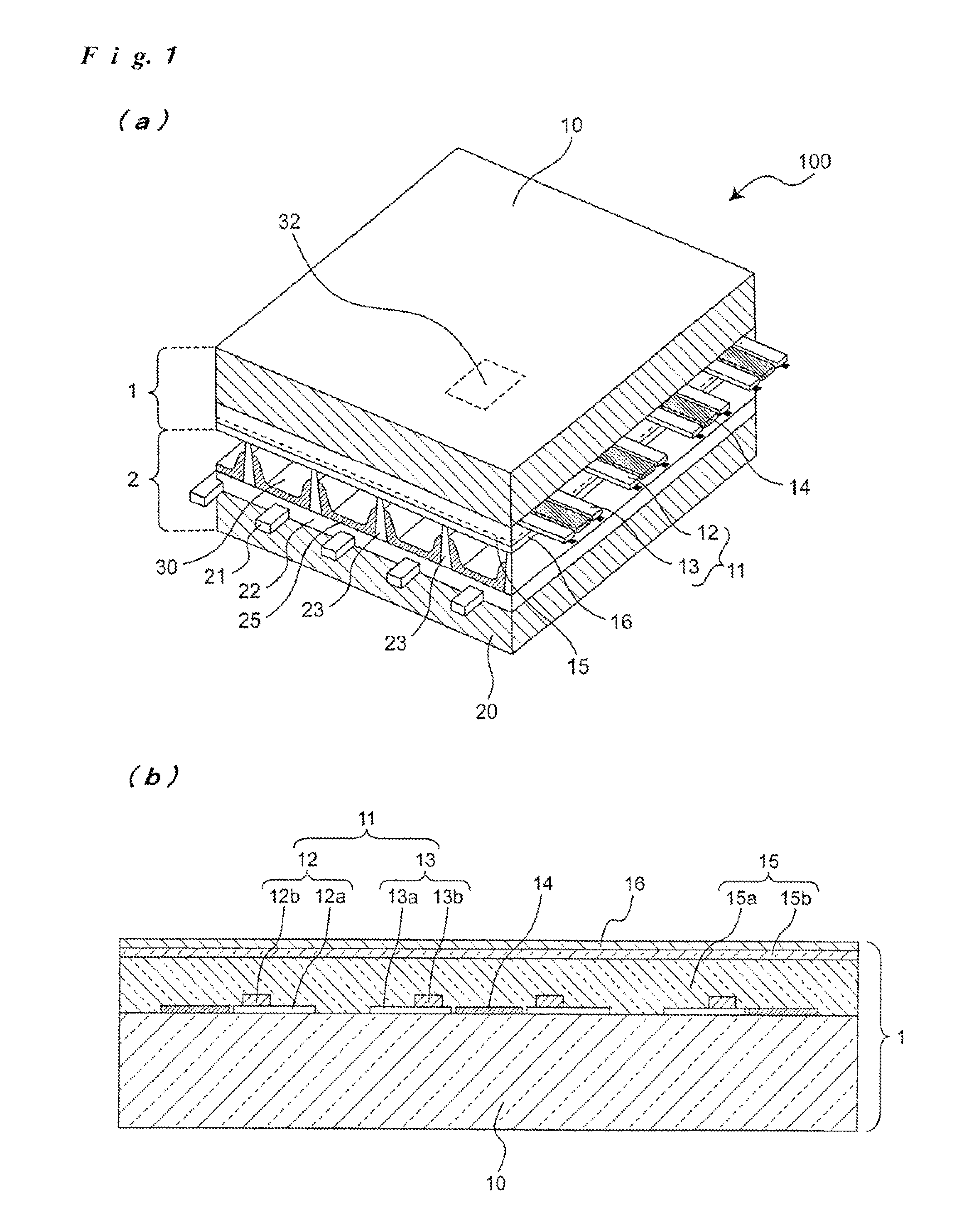
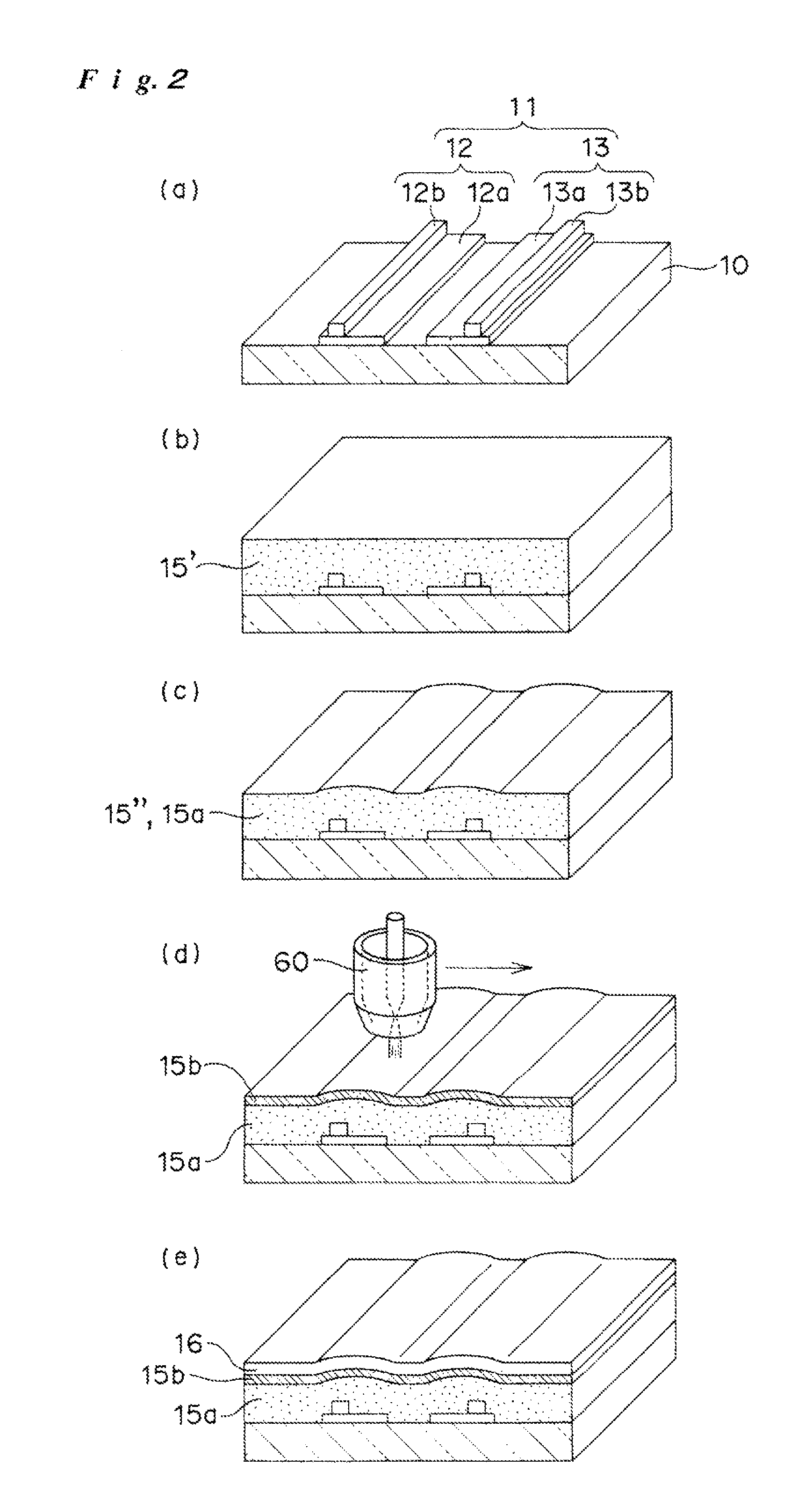
[0090]Examples of the present invention will now be described below. In the Examples, the second dielectric layer will be referred to as “cap layer” for the sake of convenience.

(Dielectric Material Paste)

[0091]Glass component (about 20% by weight with respect to entire dielectric material paste):[0092]polyalkylsiloxane oligomer, spherical amorphous silica particles (particle size: about 100 nm)[0093]Organic solvent component (about 79% by weight with respect to entire dielectric material paste):[0094]2-ethylhexanol, ethylene glycol monobutyl ether, α-terpineol[0095]Binder resin component (about 1% by weight with respect of entire dielectric material paste):[0096]Polyethylene glycol

(Production of Front Panel)

[0097]First, a transparent electrode made of ITO (about 120 μm in width and about 100 nm in thickness of the transparent electrode) was formed on a surface of 1.8 mm thick glass substrate (i.e. soda-lime glass manufactured by Nippon Electric Glass Co., Ltd.) and subsequently a bu...


PUM


Abstract

A plasma display panel includes a front panel having a dielectric layer. The dielectric layer of the front panel includes a first dielectric layer and a second dielectric layer disposed on the first dielectric layer. The gas permeability of the second dielectric layer is in the range of 0% to 1%. The second dielectric layer may be formed by heating the surface of the first dielectric layer to thermally metamorphose or transubstantiate the first dielectric layer to a limited depth from the surface the first dielectric layer.

Description

FIELD OF THE INVENTION[0001]The present invention relates to a method for producing a plasma display panel. In particular, the present invention relates to a method for producing a dielectric layer which is provided in a front panel of a plasma display panel. The present invention also relates to a plasma display panel obtained by such a method.BACKGROUND OF THE INVENTION[0002]A plasma display panel (hereinafter also referred to as “PDP”) is suitable for displaying a high-quality television image on a large screen. Thus, there has been an increasing need for various kinds of display devices using the plasma display panel.[0003]The PDP (for example, 3-electrode surface discharge type PDP) comprises a front panel facing the viewer and a rear panel opposed to each other. The front panel and the rear panel are sealed along their peripheries by a sealing material. Between the front panel and the rear panel, there is formed a discharge space filled with a discharge gas (helium, neon or th...

Claims


Application Information

Patent Timeline
IPC IPC(8): H01J17/49H01J9/02H01J11/12H01J11/22H01J11/24H01J11/26H01J11/34H01J11/38
CPCH01J9/02H01J11/12H01J11/38
Inventor KUROMIYA, MICHIRUOKUMURA, TOMOHIROHATANAKA, MOTOI
Owner PANASONIC CORP
Why Eureka
Try Eureka