Method to improve indium bump bonding via indium oxide removal using a multi-step plasma process

a plasma process and indium oxide technology, applied in the direction of layered products, chemistry apparatus and processes, cleaning using liquids, etc., can solve the problems of high yield, difficult to obtain a reliable, high yield process for high density pattern of bumps, and the tendency of indium bumps to oxidize during air exposure,

Inactive Publication Date: 2012-04-24
NASA
View PDF4 Cites 24 Cited by
  • Summary
  • Abstract
  • Description
  • Claims
  • Application Information

AI Technical Summary

Benefits of technology

[0013]According to the present invention, the above-described and other objects are accomplished by providing a unique multi-step plasma process to remove indium oxide from indium bumps. The process does not require the use of halogens, does not change the bump morphology, and shows an improvement over a single step plasma based hydrogen treatment.

Problems solved by technology

However, obtaining a reliable, high yield process for high density patterns of bumps can be quite difficult.
One problem, in particular, is the tendency of the indium bumps to oxidize during exposure to air.
The length of air exposure may vary during fabrication, and so there can be a great deal of variability in the amount of oxidation.
Unfortunately, this approach is somewhat limited.
In addition, wet chemical processes are isotropic, meaning that they will attack the bump from all sides.
This process can cause the bumps to be undercut.
This undercutting results in a lack of mechanical stability prior to bonding.
Unfortunately, from the center graph it can be seen that the reduction of indium oxide to indium metal in molecular hydrogen requires temperatures in excess of 380 degrees C. to achieve a reasonable reaction rate.
These high temperatures are often not compatible with the types of devices that are typically hybridized.
However, a single-step plasma-based hydrogen process for removing indium oxide from the indium bumps as disclosed does not completely reduce the oxide.

Method used


Image

  • Method to improve indium bump bonding via indium oxide removal using a multi-step plasma process
  • Method to improve indium bump bonding via indium oxide removal using a multi-step plasma process
  • Method to improve indium bump bonding via indium oxide removal using a multi-step plasma process

Examples


Embodiment Construction

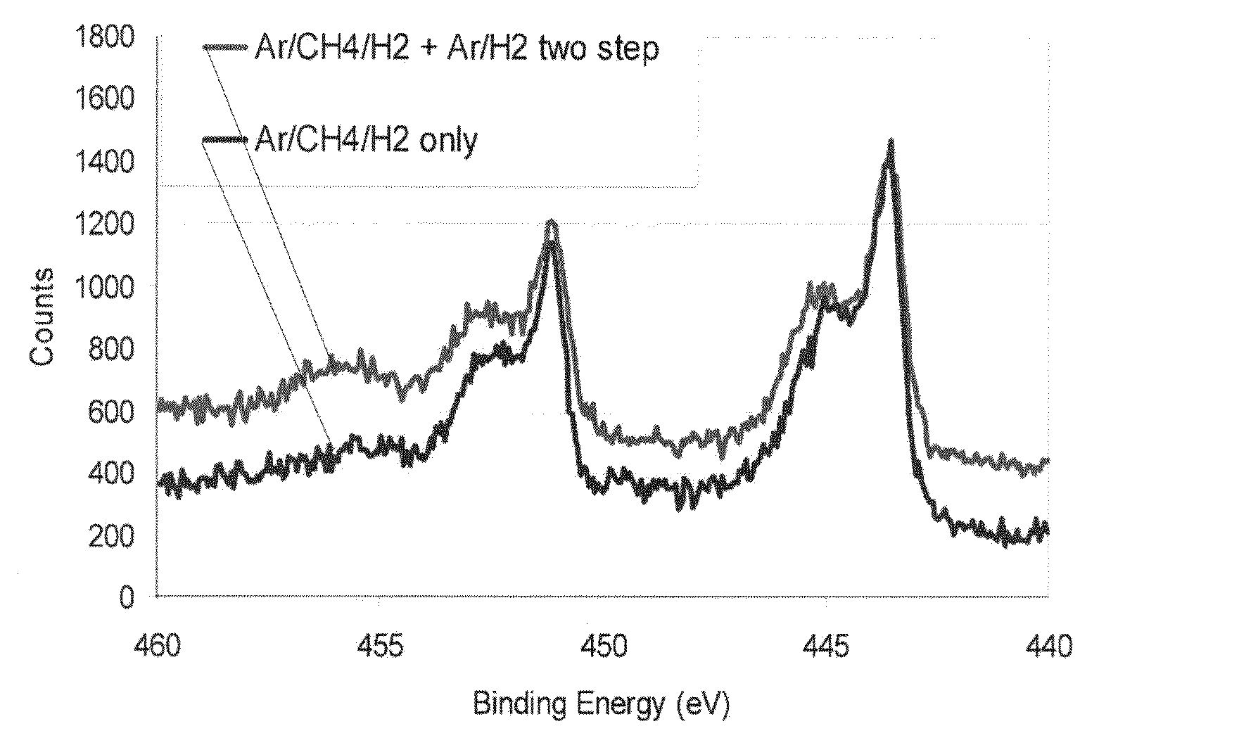
[0025]Bump bonding uses indium bumps to directly connect a semiconductor IC to another structure or substrate face down eliminating the need for wire bonding. However, if the indium bumps become oxidized prior to bump bonding a treatment is needed to remove the oxide in order to reduce the contact resistance of the solder joint between the two halves of the flip-chip structure. The present invention is a multi-step plasma process to remove indium oxide from indium bumps which does not require the use of halogens, does not change the bump morphology, and which exhibits increased removal effectiveness over a single step plasma based hydrogen treatment.

[0026]The process is intended for use on a semiconductor device having integrated circuit(s) and contact pads metalized on the surface of the device, and indium solder dots or bumps deposited on each of the pads by any conventional deposition process. Although the method of the present invention may be used with solder bumps formed by an...


PUM

PropertyMeasurementUnit
pressureaaaaaaaaaa
poweraaaaaaaaaa
pressureaaaaaaaaaa

Abstract

A process for removing indium oxide from indium bumps in a flip-chip structure to reduce contact resistance, by a multi-step plasma treatment. A first plasma treatment of the indium bumps with an argon, methane and hydrogen plasma reduces indium oxide, and a second plasma treatment with an argon and hydrogen plasma removes residual organics. The multi-step plasma process for removing indium oxide from the indium bumps is more effective in reducing the oxide, and yet does not require the use of halogens, does not change the bump morphology, does not attack the bond pad material or under-bump metallization layers, and creates no new mechanisms for open circuits.

Description

STATEMENT OF GOVERNMENT INTEREST[0001]The invention described hereunder was made in the performance of work under a NASA contract, and is subject to the provisions of Public Law #96-517 (35 U.S.C. 202) in which the Contractor has elected not to retain title.BACKGROUND[0002]a. Field of Invention[0003]The invention relates to electronic device fabrication processes and, more particularly to a process for removing indium oxide from indium bumps used in flip chip hybridization (“bump bonding”).[0004]b. Background of the Invention[0005]Flip chip hybridization, also known as bump bonding or Controlled Collapse Chip Connection (C4), is an efficient method for connecting semiconductor devices using solder bumps deposited onto their contact pads. The semiconductor device is fabricated by forming integrated circuit(s) on a wafer. Contact pads are then metalized on the surface of the ICs, and solder dots or “bumps” are deposited on each of the pads. The ICs are then cut from the wafer to form ...

Claims


Application Information

Patent Timeline
Patent Type & Authority Patents(United States)
IPC IPC(8): B08B6/00
CPCH01L24/11H01L24/13H01L2224/1181H01L2224/13109H01L2924/01005H01L2924/01006H01L2924/01013H01L2924/01033H01L2924/01041H01L2924/01049H01L2924/01074H01L2924/01075H01L2924/01077H01L2924/01078H01L2924/014H01L2924/14H01L2924/00
Inventor GREER, H. FRANKJONES, TODD J.VASQUEZ, RICHARD P.HOENK, MICHAEL E.DICKIE, MATTHEW R.NIKZAD, SHOULEH
Owner NASA
Why Eureka
Try Eureka