Structure of a pHEMT transistor capable of nanosecond switching

a technology of phemt transistor and structure, which is applied in the direction of basic electric elements, electrical apparatus, and semiconductor devices, can solve the problems of conventional phemt structure, and achieve the effects of minimizing switching delays, shortening device gate lag times, and minimizing switching delays

Active Publication Date: 2012-05-08
MACOM TECH SOLUTIONS HLDG INC
View PDF5 Cites 8 Cited by
  • Summary
  • Abstract
  • Description
  • Claims
  • Application Information

AI Technical Summary

Benefits of technology

[0007]The objects, features and advantages of the present invention include providing a method and / or apparatus for implementing a structure of a pHEMT transistor capable of nanosecond switching that may (i) have short device gate lag times, (ii) minimize switching delays due to ungated surface charge, (iii) minimize switching delays due to depletion region channel charges, (iv) reduce on resistance of a source-to-drain channel, (v) reduce a gate resistance without increasing a gate capacitance and / or (vi) incorporate an additional layer that enhances movement of charges through the device.

Problems solved by technology

While the rise times and the fall times are more than adequate, a difficulty with switching applications using the conventional pHEMT structures lies in a device gate lag time, or settling time, (i.e., the time for the RF envelope to increase from 90% to 98% or decrease from 10% to 2%).

Method used


Image

  • Structure of a pHEMT transistor capable of nanosecond switching
  • Structure of a pHEMT transistor capable of nanosecond switching
  • Structure of a pHEMT transistor capable of nanosecond switching

Examples


first embodiment

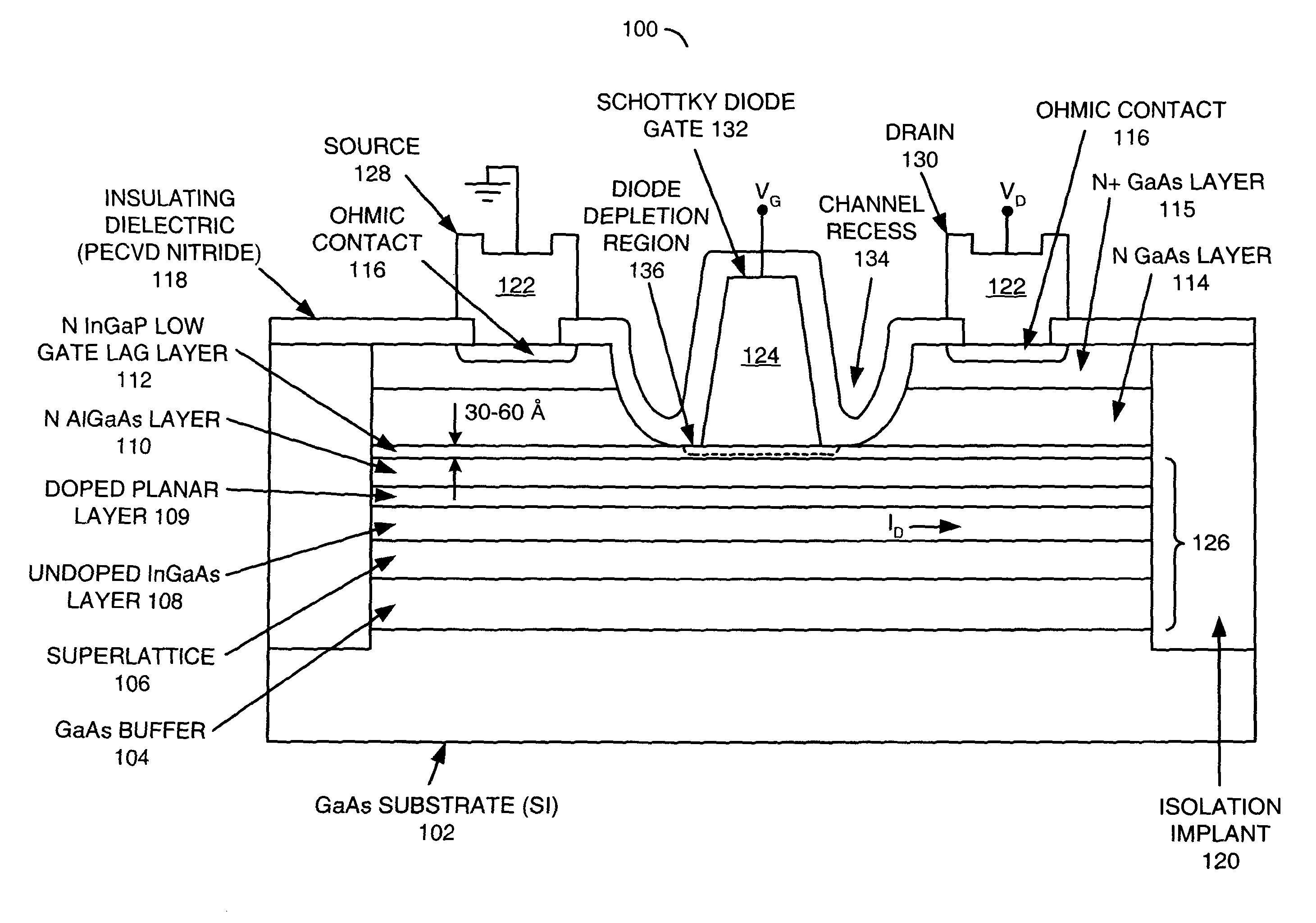
[0017]Referring to FIG. 4, a block diagram of an apparatus 100 is shown. The apparatus (or device) 100 may implement a Gallium Arsenide (GaAs) pseudomorphic High Electron Mobility Transistor (pHEMT). The apparatus 100 generally comprises a substrate (or base) 102, a layer (or region) 104, a layer (or region) 106, a layer (or region) 108, a layer (or region) 109, a layer (or region) 110, a layer (or region) 112, a layer (or region) 114, a layer (or region) 115, multiple contacts (or connections) 116, a layer (or region) 118, one or more zones (or volumes) 120, a layer (or region) 122 and a layer (or region) 124. The layers 104 to 110 may be referred to as epitaxial layers 126. The layer 122 may be patterned to create a source 128 and a drain 130 of the transistor. The layer 124 may be patterned to create a gate 132 of the transistor. A channel recess 134 may be formed in the layers 114 and 115. The gate 132 may be formed on the layer 112 within the channel recess 134. The apparatus 1...

second embodiment

[0031]Referring to FIG. 5, a cross-sectional view of an apparatus 160 is shown in accordance with a preferred embodiment of the present invention. The apparatus (or device) 160 may implement a GaAs pHEMT. The apparatus 160 generally comprises the substrate 102, the layer 104, the layer 106, the layer 108, the layer 109, the layer 110, the layer 112, the layer 114, the layer 115, the contacts 116, the layer 118, the zones 120, the layer 122 and the layer 124. The layers 104 to 110 may be referred to as the epitaxial layers 126. The layer 122 may be patterned to create the source 128 and the drain 130 of the transistor. The layer 124 may be patterned to create the gate 132a of the transistor. Two or more channel recesses 134a and 134b may be formed in the layers 114 and 115. The gate 132a may be formed on the layer 112 partially within the channel recesses 134a and 134b. The apparatus 160 is generally configured as a depletion mode device. The apparatus 160 may be normally “on” at no ...


PUM


Abstract

A method for fabricating a transistor and the resulting transistor is disclosed. The method generally includes steps (A) to (E). Step (A) may form a high mobility layer. The high mobility layer is generally configured to carry a two-dimensional electron gas. Step (B) may form a planar layer on the high mobility layer. Step (C) may form a barrier layer on the planar layer. Step (D) may form a doped layer on the barrier layer. The doped layer is generally a low bandgap III-V semiconductor. Step (E) may form a gate in contact with the doped layer. The gate may be separated from both a source and a drain by corresponding ungated recess regions. The high mobility layer, the planar layer, the barrier layer, the doped layer, the source, the gate and the drain are generally configured as a pseudomorphic high electron mobility transistor.

Description

FIELD OF THE INVENTION[0001]The present invention relates to pseudomorphic High Electron Mobility Transistors (pHEMT) generally and, more particularly, to a method and / or apparatus for implementing a structure of a pHEMT transistor capable of nanosecond switching.BACKGROUND OF THE INVENTION[0002]Referring to FIG. 1, a cross sectional view of a conventional Gallium Arsenide (GaAs) pHEMT epitaxial structure 10 is shown during fabrication. Common GaAs pHEMT transistors used in switching applications have been available for over a decade. The transistors are produced by growing epitaxial layers 12 on a semi-insulating GaAs substrate 14 utilizing either Molecular Beam Epitaxy (MBE) or Metal-Organic Chemical Vapor Deposition Epitaxy (MOCVD) techniques. An optional updoped layer 16 is sometimes included. The layer 16 serves as an etch stop for etching an upper doped GaAs layer 18 during subsequent device fabrication. However, similar performances have been achieved without the etch stop la...

Claims


Application Information

Patent Timeline
Patent Type & Authority Patents(United States)
IPC IPC(8): H01L29/778H01L21/338
CPCH01L29/42316H01L29/475H01L29/66462H01L29/7787
Inventor BOLES, TIMOTHY E.FREESTON, ANDREW K.VARMAZIS, COSTAS D.
Owner MACOM TECH SOLUTIONS HLDG INC
Why Eureka
Try Eureka