Method for manufacturing semiconductor device

a semiconductor and manufacturing technology, applied in semiconductor devices, instruments, electrical devices, etc., can solve problems such as the difference in stoichiometric composition of oxide semiconductors, and achieve the effects of stable electric characteristics, excellent electric characteristics, and high reliability

Active Publication Date: 2012-06-05
SEMICON ENERGY LAB CO LTD
View PDF131 Cites 62 Cited by
  • Summary
  • Abstract
  • Description
  • Claims
  • Application Information

AI Technical Summary

Benefits of technology

[0014]Besides impurities such as moisture existing in the oxide semiconductor film, impurities such as moisture existing in the gate insulating layer and those at interfaces between the oxide semiconductor film and upper and lower films provided in contact therewith are reduced.
[0047]A thin film transistor having stable electric characteristics can be provided. Further, a semiconductor device which includes thin film transistors having excellent electric characteristics and high reliability can be provided.

Problems solved by technology

However, a difference from the stoichiometric composition in an oxide semiconductor arises in a thin film formation process.

Method used


Image

  • Method for manufacturing semiconductor device
  • Method for manufacturing semiconductor device
  • Method for manufacturing semiconductor device

Examples


embodiment 1

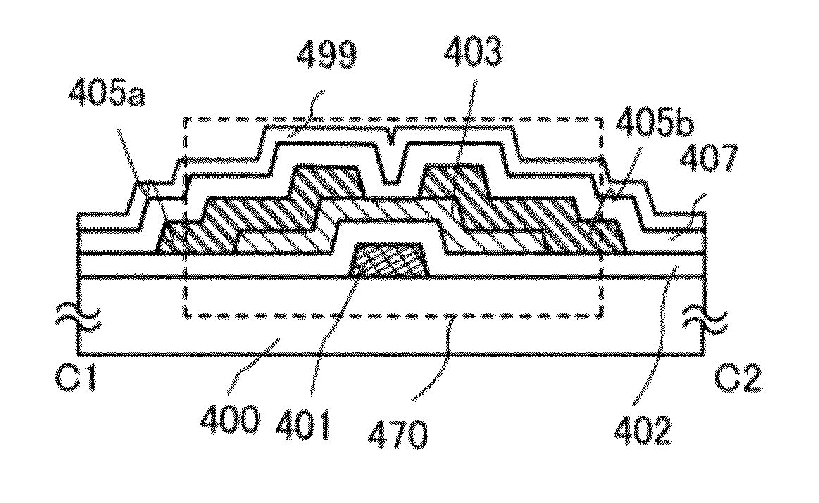
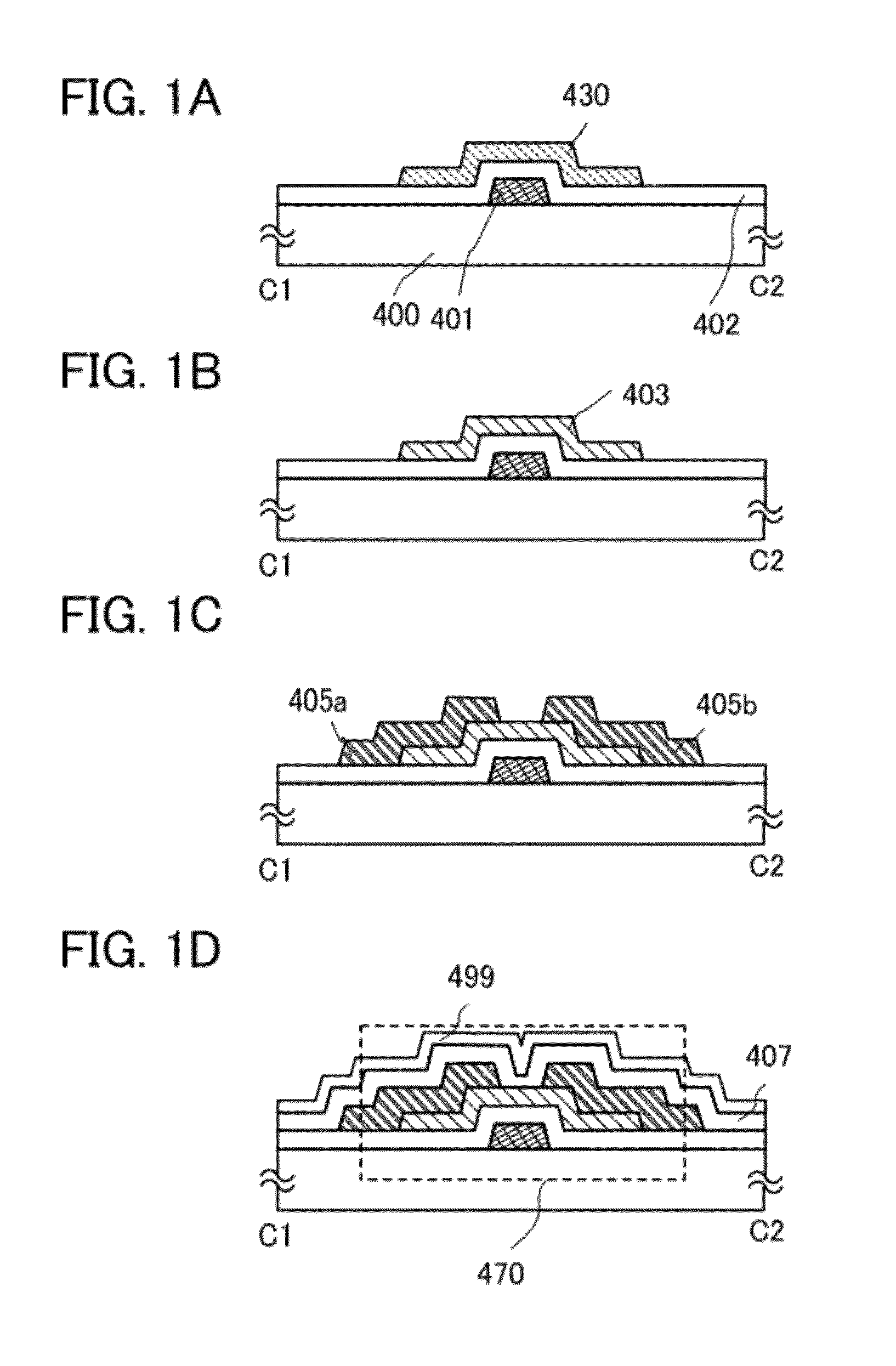
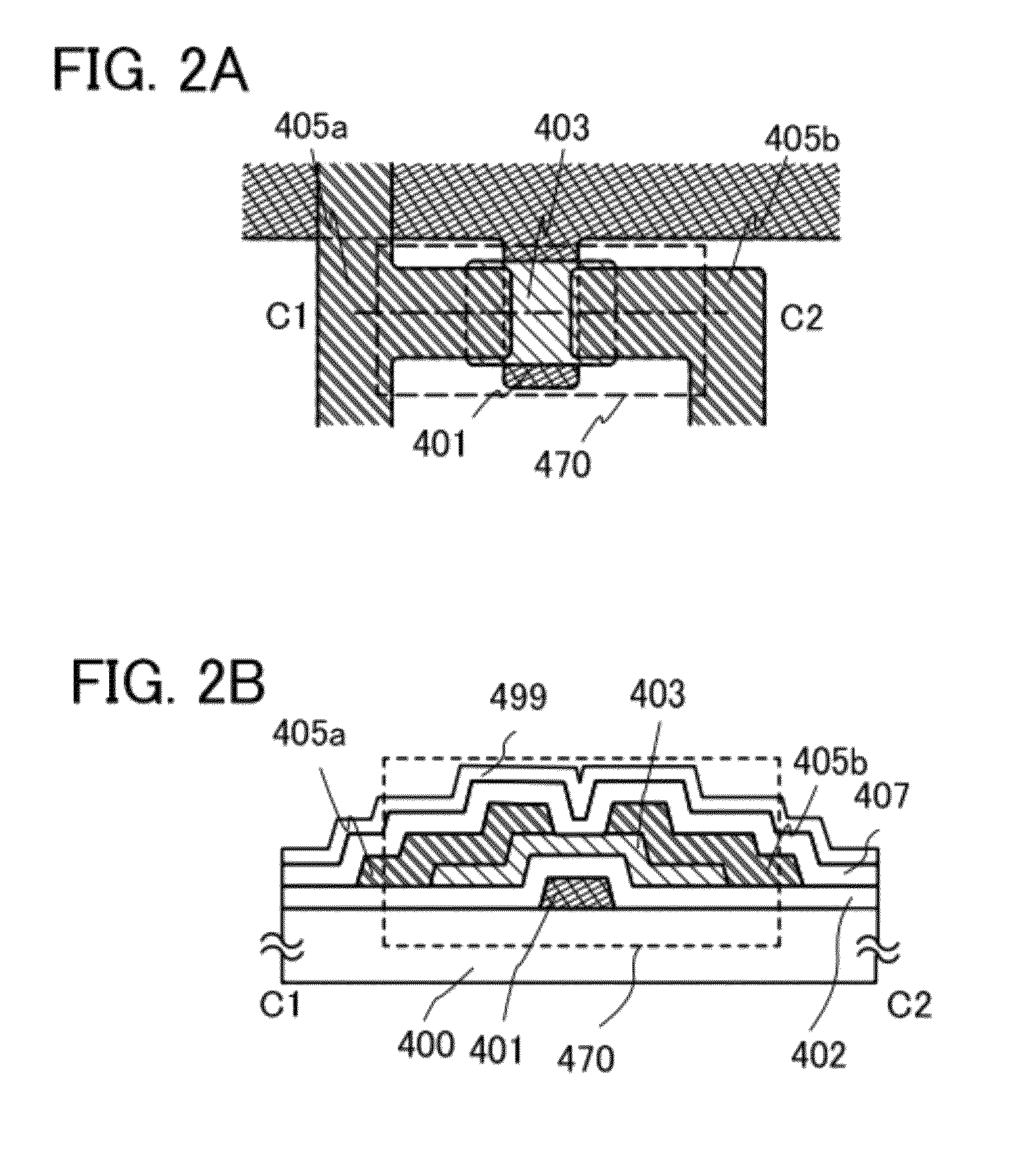
[0093]A semiconductor device and a method for manufacturing the semiconductor device will be described with reference to FIGS. 1A to 1D and FIGS. 2A and 2B.

[0094]FIG. 2A is a plan view of a thin film transistor 470 included in a semiconductor device, and FIG. 2B is a cross-sectional view taken along line C1-C2 of FIG. 2A. The thin film transistor 470 is an inverted staggered thin film transistor and includes, over a substrate 400 which is a substrate having an insulating surface, a gate electrode layer 401, a gate insulating layer 402, an oxide semiconductor layer 403, a source electrode layer 405a, and a drain electrode layer 405b. The thin film transistor 470 is covered with an insulating layer 407 which is in contact with the oxide semiconductor layer 403. A protective insulating layer 499 is stacked over the insulating layer 407.

[0095]In order to suppress variation in electric characteristics of the thin film transistor 470, impurities such as hydrogen, moisture, hydroxyl, or hy...

embodiment 2

[0198]A semiconductor device and a method for manufacturing the semiconductor device will be described with reference to FIGS. 8A to 8D and FIGS. 9A and 9B. The same portion as or a portion having a function similar to that described in Embodiment 1 can be formed in a manner similar to that described in Embodiment 1, and also the steps similar to those of Embodiment 1 can be performed in a manner similar to those described in Embodiment 1; therefore, repetitive description is omitted.

[0199]FIG. 9A is a plan view of a thin film transistor 460 included in a semiconductor device, and FIG. 9B is a cross-sectional view along line D1-D2 of FIG. 9A. The thin film transistor 460 is a bottom-gate thin film transistor and includes, over a substrate 450 which is a substrate having an insulating surface, a gate electrode layer 451, a gate insulating layer 452, source or drain electrode layers 455a and 455b, and an oxide semiconductor layer 453. The thin film transistor 460 is covered with an in...

embodiment 3

[0232]This embodiment describes an example of a channel-stop-type thin film transistor, using FIGS. 34A, 34B, and 34C. FIG. 34C illustrates an example of a top view of the thin film transistor, cross-sectional view along dotted line Z1-Z2 of which corresponds to FIG. 34B. The same portion as or a portion having a function similar to that described in Embodiment 1 can be formed in a manner similar to that described in Embodiment 1, and also the steps similar to those of Embodiment 1 can be performed in a manner similar to those described in Embodiment 1; therefore, repetitive description is omitted.

[0233]As in FIG. 34A, a gate electrode layer 1401 is formed over a substrate 1400. Next, an oxide semiconductor layer is formed over a gate insulating layer 1402 covering the gate electrode layer 1401.

[0234]In this embodiment, a Sn—Zn—O-based oxide semiconductor layer formed by a sputtering method is used for an oxide semiconductor layer 1403.

[0235]Heat treatment for dehydration or dehydro...


PUM

PropertyMeasurementUnit
dew pointaaaaaaaaaa
gate voltageaaaaaaaaaa
dew pointaaaaaaaaaa

Abstract

An object is to provide a semiconductor device having stable electric characteristics in which an oxide semiconductor is used. An oxide semiconductor layer is subjected to heat treatment for dehydration or dehydrogenation treatment in a nitrogen gas or an inert gas atmosphere such as a rare gas (e.g., argon or helium) or under reduced pressure and to a cooling step for treatment for supplying oxygen in an atmosphere of oxygen, an atmosphere of oxygen and nitrogen, or the air (having a dew point of preferably lower than or equal to −40° C., still preferably lower than or equal to −50° C.) atmosphere. The oxide semiconductor layer is thus highly purified, whereby an i-type oxide semiconductor layer is formed. A semiconductor device including a thin film transistor having the oxide semiconductor layer is manufactured.

Description

TECHNICAL FIELD[0001]The present invention relates to a semiconductor device including an oxide semiconductor and a method for manufacturing the semiconductor device.[0002]In this specification, a semiconductor device generally means a device which can function by utilizing semiconductor characteristics, and an electro-optic device, a semiconductor circuit, and electronic equipment are all semiconductor devices.BACKGROUND ART[0003]A technique for forming a thin film transistor (TFT) by using a thin semiconductor film formed over a substrate having an insulating surface has attracted attention. A thin film transistor is used for a display device typified by a liquid crystal television. A silicon-based semiconductor material is known as a material for a thin semiconductor film applicable to a thin film transistor. As another material, an oxide semiconductor has attracted attention.[0004]As a material of the oxide semiconductor, zinc oxide or a material including zinc oxide as its comp...

Claims


Application Information

Patent Timeline
Patent Type & Authority Patents(United States)
IPC IPC(8): H01L21/00
CPCH01L21/02554H01L21/02565H01L21/02631H01L21/02107H01L29/7869H01L29/66969H01L27/1225H01L21/324H01L29/4908H01L29/66742H01L21/02266G02F1/133302G02F1/133531H10K59/1213H01L21/02672G02F1/133528G02F1/1339G02F1/134336G02F1/136286G02F1/1368G02F2201/121G02F2201/123G09G3/3677G09G2310/0286G09G2310/08H01L21/477H01L21/67115H01L27/127H01L29/78696
Inventor HOSOBA, MIYUKISAKATA, JUNICHIROOHARA, HIROKIYAMAZAKI, SHUNPEI
Owner SEMICON ENERGY LAB CO LTD
Why Eureka
Try Eureka