Near field detection for optical metrology

a near field detection and metrology technology, applied in the field of optical metrology, can solve the problems of limited spatial resolution, limited wavelength range resolution, and large wavelength of relevant spectral bands, and achieve the effects of fewer scanning steps, different widths, and more information about the targ

Active Publication Date: 2012-06-26
KLA CORP
View PDF18 Cites 10 Cited by
  • Summary
  • Abstract
  • Description
  • Claims
  • Application Information

AI Technical Summary

Benefits of technology

[0034]By placing the near field optical probe in the central obscuration of the objective, embodiments of the present invention allow images of the target to be obtained quickly so that areas of interest can be located. If these areas of interest contain small-scale features, the near field optical probe can be brought into proximity to the target for near field probe measurements. Such a system combines the best features of far field and near field optical techniques into a single tool.
[0040]FIG. 2B is a schematic diagram illustrating operation of a near field optical probe of the type shown in FIG. 1 in a reflection mode. As shown in FIG. 2B, an optical cavity 202, light source 204 and detector 206, can all be optically coupled by optical fibers 201A, 201B, 203 respectively to an optical coupler 205. Radiation from a source 204 can be coupled to and from the optical cavity 202 via the optical coupler 205 and fiber 203. A small opening in the cavity202 allows evanescent waves E to optically couple energy from propagating states in the cavity 202 to a target 208. Changes in the propagating states in the optical cavity 202 can be detected at the detector 206, e.g., in terms intensity, wavelength, polarization or phase. The detector 206 can produce a difference signal corresponding to these changes. The difference signal from the detector 206 can be coupled to an analyzer 210, e.g., a special purpose computer or suitably programmed general purpose computer. The analyzer 210 can be configured to determine properties of the target 208 from the difference signal. The analyzer 210 can optionally receive signals obtained from radiation emanating from the source 204 to measure differences in radiation coupled to and from the cavity 202.
[0041]The configuration shown in FIG. 2B can be used to make measurements similar to those described above with respect to FIG. 2A. The configuration shown in FIG. 2B has an advantageous optical system design due to the use of a single fiber 203 to couple light to and from the optical cavity 202. The use of a single fiber facilitates background rejection. As in the configuration shown in FIG. 2A, Z scan can support film thickness measurement in a configuration like the one shown in FIG. 2B.
[0051]The near field probe can be mounted to the same mechanical structure as the objective. By mounting the probe in this way, an existing optical tool can be readily modified to add a scanning probe capability. For example, many inspection and metrology tools include a stage for mounting the sample. The stage often includes a mechanism for translating or rotating the target. This mechanism can be used to scan the target in the X and Y directions. The tool may also include a Z translation mechanism to allow translation of the stage along a Z direction that is perpendicular to the X and Y directions. Such a capability is often included to facilitate focusing of the objective of the target. This Z-translation capability can be incorporated into the target stage or into the mounting of the objective or an entire optical column of which the objective is a part. This mechanism can be used to bring the near field probe into sufficient proximity to the target to allow coupling of evanescent waves for NSOM.
[0053]By way of example, and not by way of limitation, a near field optical probe can be combined with an optical metrology or inspection tool that employs a reflective or catadioptric objective. In this case, the optical cavity of the near field probe can be located in the objective's central obscuration, when not needed and brought into proximity to the target when required. Such a configuration can save space as well as time of the navigation step as the near field device is already above the target measured previously by the method using the reflective objective. In some implementations the optical tool may include a reflective objective for the purpose of navigating the near field probe over the target, which can be a challenge for near field probes.
[0084]The use of near field based metrology in combination with existing optical metrology and inspection techniques opens a new realm of opportunities for accurate nanometer scale metrology as by combining the maturity and flexibility of optical technologies with the capability of measuring deeply sub-wavelength features.

Problems solved by technology

One of the main obstacles in achieving these metrology requirements with optical based technologies is the large wavelength of the relevant spectral bands and the consequent limited resolution.
These limitations are relevant to common far field technologies.
Conventional optical metrology methods are based on propagating optical waves and as such are limited by wavelength range resolutions.
Unfortunately, in an optical system operating in a far-field mode, the spatial resolution is diffraction limited.
The diffraction limit in traditional optics is imposed by the use of propagating waves in the imaging process.
However, a key difference between a conventional SEM and an optical microscope is that an SEM must operate with the target under vacuum.
This can slow down the rate at which an SEM can inspect or measure different wafers and also makes an SEM system more expensive and complex.
Unfortunately, such coatings may alter the target, e.g., by obscuring very small scale features.
Furthermore, scanning probe technologies, such as Atomic Force Microscope (AFM), Scanning Tunneling Microscope (STM) and electronic microscope, are best suited for measuring two-dimensional information and have limited ability to provide three-dimensional information.
In addition, the measurement and imaging process with scanning probe tools is slow.

Method used


Image

  • Near field detection for optical metrology
  • Near field detection for optical metrology
  • Near field detection for optical metrology

Examples


embodiments

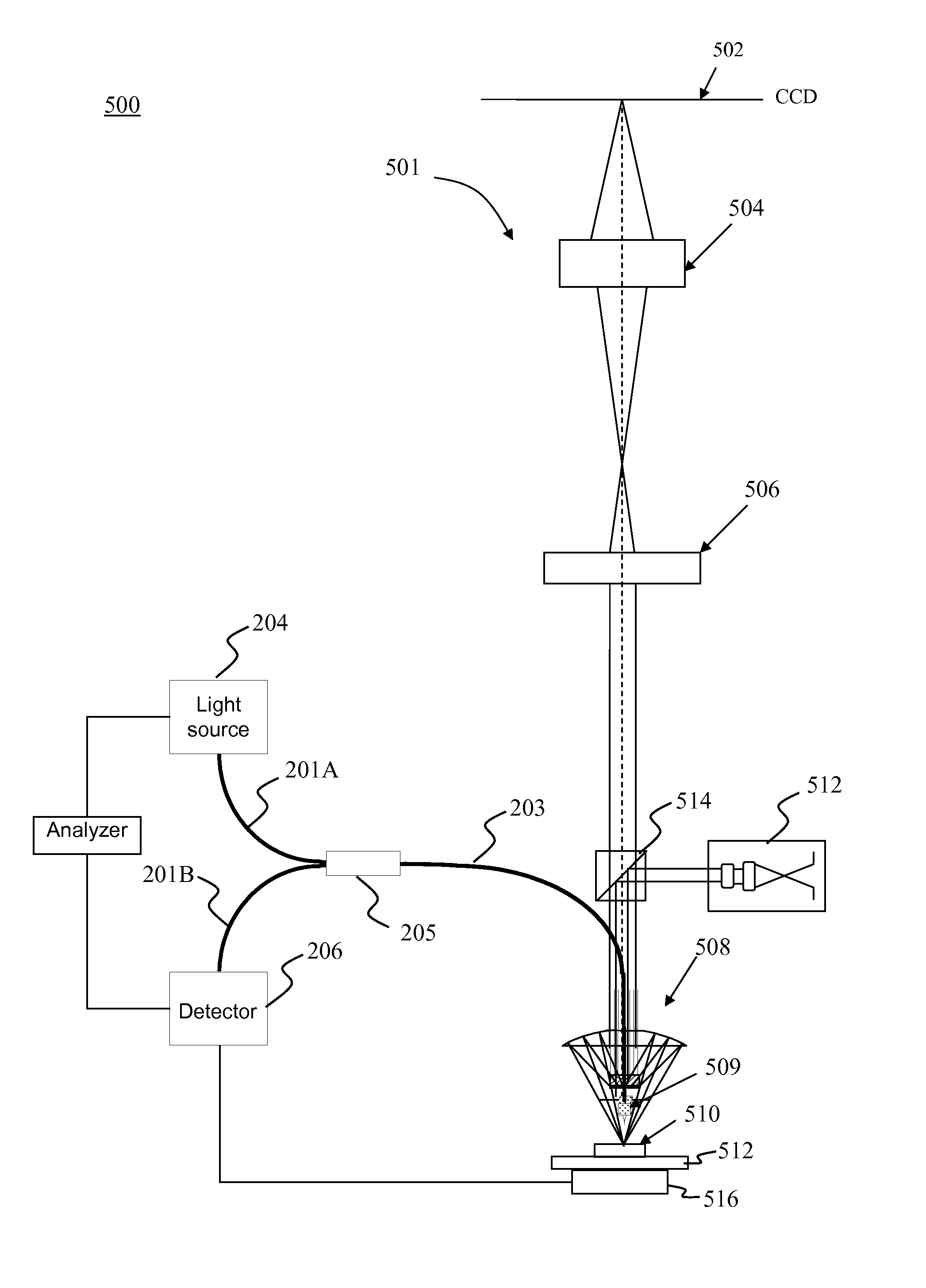
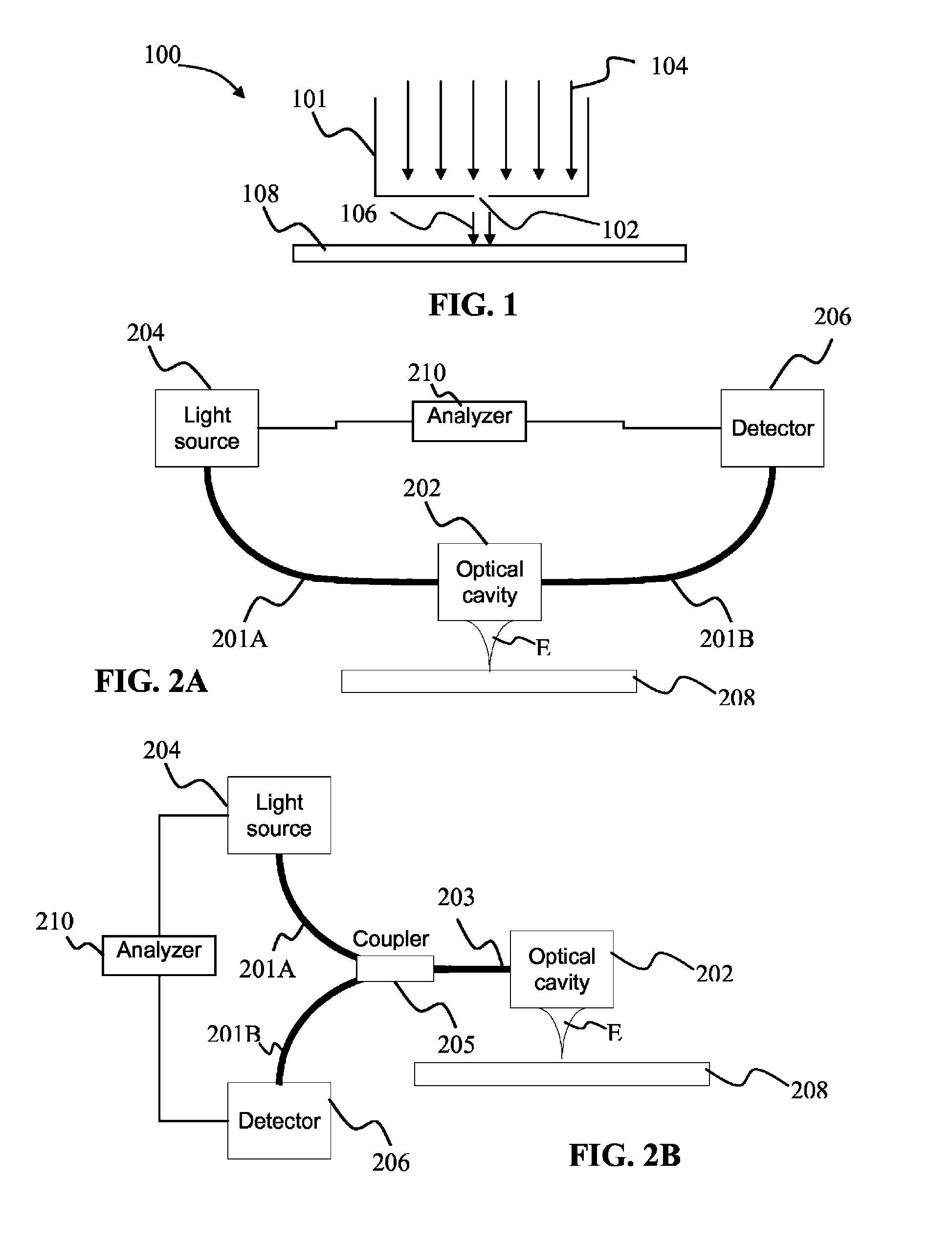
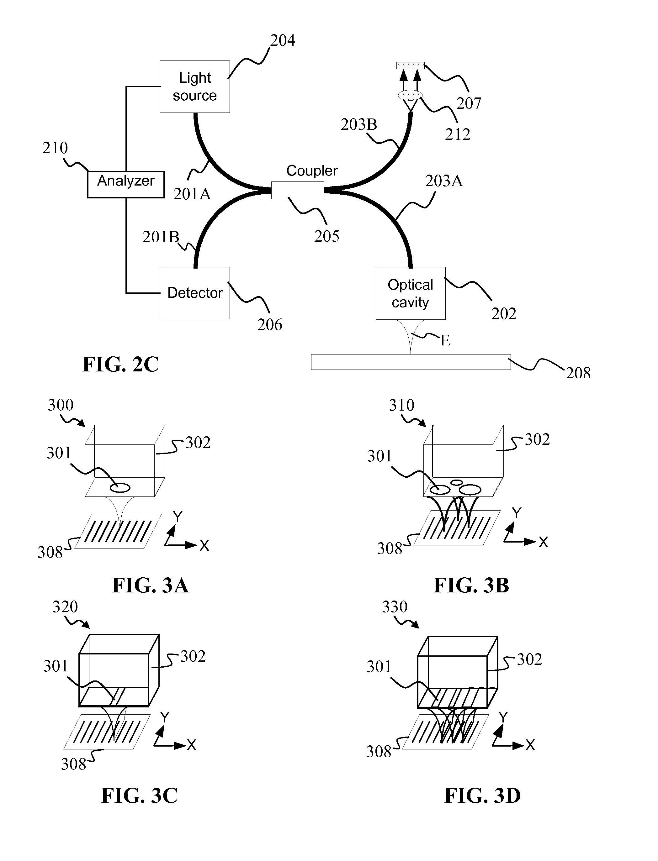
[0032]In an embodiment of the present invention, a near field optical probe is located within the central obscuration of the objective of an optical metrology or inspection tool. The near field optical probe includes an optical cavity with at least one opening configured to face a target. A width of the opening is smaller than the wavelength of the electromagnetic radiation. The near field optical probe includes a mechanism configured to bring the optical cavity into proximity to the target.

[0033]When the optical cavity is brought into sufficient proximity to a target evanescent optical waves emanating from the cavity through the opening can be coupled to both the target and a propagating wave inside the cavity. Interaction between the evanescent wave and the target can change in the coupling between the near field radiation and the propagating wave. Changes in the coupling between the near field wave and the propagating wave can be detected. This technique can detect changes in a m...


PUM

PropertyMeasurementUnit
thicknessaaaaaaaaaa
thickaaaaaaaaaa
sub-wavelength aaaaaaaaaa

Abstract

An optical metrology tool may include a source of electromagnetic radiation having a characteristic wavelength, an objective having a central obscuration, a near field element located within the central obscuration of the objective, and an electromagnetic radiation detector coupled to the near field element. A mechanism is configured to bring the near field element into proximity to the target. A characteristic dimension of the near field element is sufficient smaller than the wavelength of the electromagnetic radiation that when the electromagnetic radiation passes through the cavity and the cavity is in sufficient proximity to the target that evanescent waves can couple energy from propagating radiation in the near-field element to the target. The detector detects an optical signal due to the evanescent waves coupling to the target.

Description

FIELD OF THE INVENTION[0001]This invention generally relates to optical metrology and more particularly to implementing optical near field detection for optical metrology.BACKGROUND OF THE INVENTION[0002]The semiconductor industry often uses far field optical imaging tools such as microscopes or scatterometers for wafer inspection and metrology. Such tools typically couple light from a source to a target through an objective lens. Light scattered from the target is coupled back through the objective to an imaging detector via an optical column. Such far-field optical tools can operate quite quickly and can obtain three-dimensional information about a target.[0003]Another class of imaging tools includes electron microscopes, such as the scanning electron microscope (SEM). The SEM can form an image of a target using an electron beam instead of light. The SEM operates in a similar manner to an optical microscope. Instead of an optical beam, an electron beam is coupled to the target thr...

Claims


Application Information

Patent Timeline
Patent Type & Authority Patents(United States)
IPC IPC(8): G02F1/01G01J4/00
CPCG01B11/026G01Q60/22B82Y35/00B82Y20/00
Inventor MANASSEN, AMNON
Owner KLA CORP
Why Eureka
Try Eureka