Wiring structure and electronic device designed on basis of electron wave-particle duality

a wiring structure and electronic device technology, applied in the field of wiring structure and electronic device design on the basis of electron wave-particle duality, can solve the problems of increasing the resistance of the ic and the lsi circuit, increasing the heat generation and deterioration of the signal waveform, and increasing the resistance of the lsi circuit. achieve the effect of saving an enormous amount of energy

Active Publication Date: 2012-08-28
SUZUKI CO LTD Y
View PDF9 Cites 0 Cited by
  • Summary
  • Abstract
  • Description
  • Claims
  • Application Information

AI Technical Summary

Benefits of technology

[0018]When the wiring structure and the electronic device such as an LSI circuit etc. of the present invention are used on the assumption that the electric power consumption of them is lowered even by several percents as compared with the present situation, then it is possible to save an enormous amount of the energy in all over the world.

Problems solved by technology

In a macroscopic viewpoint as well, this fact results in an increase in the resistance of the IC and the LSI circuit.
Therefore, the heat generation is caused thereby, and the rising and falling characteristics of individual signals are deteriorated.
The more the width of the wiring structure becomes narrow, the more the bent corner of the wiring structure especially tends to cause the heat generation.
Therefore, even when the electron comes toward the joining surface, then the electron not necessarily pass therethrough successfully once, and the electron repeats the reflection and the reentry several times. If the number of times of the incidence and the reflection is increased, then the stay of electrons arises, and this situation results in a larger amount of the heat generation and the deterioration of the signal waveform.

Method used


Image

  • Wiring structure and electronic device designed on basis of electron wave-particle duality
  • Wiring structure and electronic device designed on basis of electron wave-particle duality
  • Wiring structure and electronic device designed on basis of electron wave-particle duality

Examples


first embodiment

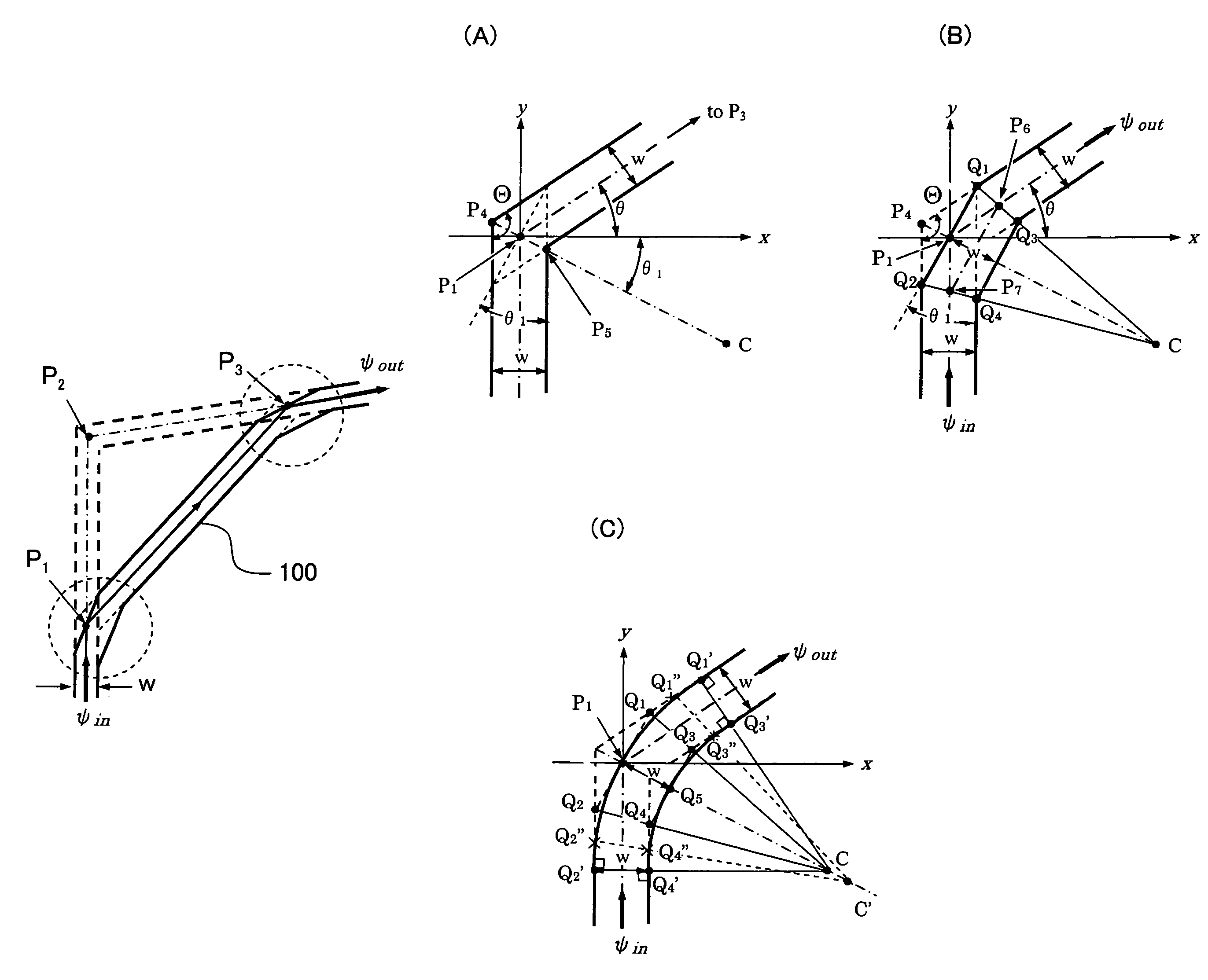
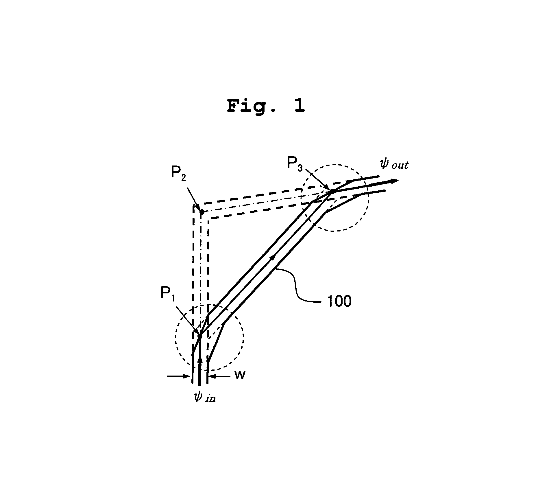
[0041]In the case of a straight wiring structure which is linearly symmetrical in relation to the center line, electrons travel in the direction of the center line of the wiring structure in average in accordance with the electric potential gradient in the wiring structure. The average direction of motion of the electrons is coincident with the direction of the center line. Therefore, the average de Broglie wave, which precedes the electrons, goes straight ahead while allowing the wave number vector stands at the center of the wavefront to coincide with the center line. More simply speaking, the average de Broglie wave can be represented by a single light ray which goes straight ahead on the center line. However, the light ray in this case is different from any ordinary light ray, because the propagation velocity exceeds the velocity of light. When bent corners and / or branched portions of wiring structures are designed, in general, an important guideline is to minimize the number of...

second embodiment

[0074]Even when the signal transmission characteristic is improved for only wiring portions of an LSI circuit, if the stay of electrons occurs at a connecting surface between the wiring portion and each of the devices such as the transistors incorporated into the LSI circuit, then the effect of the improvement of the wiring portion is consequently suppressed. Further, in order to improve the characteristic of the entire LSI circuit, it is also necessary to improve the signal transmission characteristic at the boundary surface between materials of different types in each of the devices. An explanation will be made below with reference to FIGS. 10 to 15 about a method for improving the signal transmission characteristic at the boundary surface between the materials of the different types as described above, by applying the concept of the simultaneous duality consisting of electrons and an average de Broglie wave which precedes the electrons.

[0075]FIG. 10A shows a sectional view illust...


PUM


Abstract

According to a simultaneous duel model that a de Broglie wave accompanies an electron drift-moving in an electron circuit, wiring is considered as a waveguide of the average de Broglie wave and design was performed by reducing the resistance value at bending portion of the wiring. Furthermore, by providing a micro-structure having a wave suppressing function of average de Broglie wave on the boundary between the metal electrode and the semiconductor electrode, so that electron transmitting probability at the boundary is increased. This improves electric feature of a macro structure portion which may cause a local heating such as a bending corner of wiring contained in the electronic circuit such as an IC and an LSI or a boundary between the metal electrode and the semiconductor electrode.

Description

TECHNICAL FIELD[0001]The present invention relates to a wiring structure designed by such a method that a macroscopic structure portion, which is possessed by an electronic circuit such as an IC and an LSI circuit, is designed on the basis of the microscopic property possessed by each of individual electrons, i.e., the wave-particle duality. Further, the present invention relates to an electronic device designed by using such a designing method and then produced.BACKGROUND ART[0002]The field of the study in relation to the physical properties of, for example, the dielectric substance, the magnetic substance, and the semiconductor is called “solid state physics”. Quantum mechanics lies in the basis thereof. However, the wave nature of individual electrons has not been hitherto applied to design the macroscopic structure portion possessed by the electronic circuit including the semiconductor such as the IC and the LSI circuit. The macroscopic structure portion of the electronic circui...

Claims


Application Information

Patent Timeline
Patent Type & Authority Patents(United States)
IPC IPC(8): H01L21/302
CPCG06F17/5077H01L23/528H01L2924/0002H01L2924/00G06F30/394
Inventor SUZUKI, TAKASHI
Owner SUZUKI CO LTD Y
Why Eureka
Try Eureka