Electrostatic chuck device

a technology of electrostatic chuck and chuck body, which is applied in the direction of electrostatic holding device, manufacturing tools, mechanical equipment, etc., can solve the problems of insufficient action and responsiveness of electrostatic adsorption force, inability to obtain processing, and insufficient plasma process in-plane unevenness, so as to achieve superior action and responsiveness, superior density and mechanical strength, the effect of uniform plasma density

Active Publication Date: 2012-09-11
SUMITOMO OSAKA CEMENT CO LTD
View PDF10 Cites 0 Cited by
  • Summary
  • Abstract
  • Description
  • Claims
  • Application Information

AI Technical Summary

Benefits of technology

[0039]According to the electrostatic chuck device of the present invention, because the electrostatic-absorption inner electrode is formed by a complex sintered body that contains insulating ceramics and silicon carbide and the volumetric resistance thereof is set within a range of 1.0×10⁻¹ Ωcm to 1.0×10⁵ Ωcm, even if the content of the silicon carbide (SiC), which is the conducting component, deviates from the content that is necessary for obtaining the target volumetric resistance, and in addition, even if the heat treatment temperature and the baking temperature vary when fabricating this electrostatic-adsorption inner electrode, the volumetric resistance of this electrostatic-adsorption inner electrode can be advantageously maintained within a range of 1.0×10⁻¹ Ωcm to 1.0×10⁵ Ωcm. Therefore, when high frequency voltage is applied to the metal base, a high frequency current can pass through the electrostatic-adsorption inner electrode, and a uniform plasma density can be effectively attained.
[0040]Thus, a uniform plasma process can be applied to the plate-like sample. In addition, an electrostatic adsorption force having superior action and responsiveness can be attained.
[0041]In addition, because the complex sintered body contains silicon carbide in a range of 5 wt % to 20 wt %, the volumetric resistance of the electrostatic-adsorption inner electrode can be easily controlled so as to be within a range of 1.0×10⁻¹ Ωcm to 1.0×10⁵ Ωcm.
[0042]In addition, because the complex sintered body contains silicon carbide, a superior density and mechanical strength can be imparted thereto.
[0043]In addition, because the complex sintered body contains one or more species selected from a group consisting of metals, carbon, and conducting ceramics equal to or less than a total of 30 vol %, the volumetric resistance can be easily prepared so as to be within a range of 1.0×10⁻¹ Ωcm to 1.0×10⁵ Ωcm.

Problems solved by technology

Accordingly, when the distribution of the electric field strength is not even, the electron density of the generated plasma is not even and thus the processing rate varies depending on in-plane positions in the plate-like sample W. Therefore, there is a problem in that it is not possible to obtain a processing result excellent in in-plane uniformity.
However, even in such an electrostatic chuck device, because the potential of the plasma above the center portion of the plate-like sample W becomes high and the potential at the peripheral portion thereof becomes low, the processing rate differs at the center portion and the peripheral portion of the plate-like sample W, and there is a problem in that this is a factor causing in-plane unevenness in a plasma process such as etching.
In addition, the action and responsiveness of the electrostatic adsorption force were also inadequate.
However, when fabricating the electrostatic-adsorption inner electrode by using the sintered bodies in (1) to (3) described above, it is difficult to evenly mix conducting components such as high melting temperature metals, conducting ceramics, and carbon, with insulating ceramics on an industrial scale.
Thus, the proportions of these conducting components easily deviate from the proportions that are necessary for obtaining the target volumetric resistance value.
Thus, this volumetric resistance does not attain a desired constant value, and therefore there is a problem in that the volumetric resistance easily deviates from a range of 1.0×10⁻¹ Ωcm to 1.0×10⁵ Ωcm, and preferably, from 1.0×10² Ωcm to 1.0×10⁴ Ωcm, and preparing the volumetric resistance of the electrostatic-adsorption inner electrode so as to attain the desired constant value is extremely difficult.
Thus, this volumetric resistance does not attain the desired constant value, and therefore there is a problem in that the volumetric resistance easily deviates from the range of 1.0×10⁻¹ Ωcm to 1.0×10⁵ Ωcm, and preferably, from 1.0×10² Ωcm to 1.0×10⁴ Ωcm, and preparing the volumetric resistance of the electrostatic-adsorption inner electrode so as to attain a desired constant value becomes extremely difficult.
Accordingly, the volumetric resistance of the electrostatic-absorption inner electrode is easily influenced by the variations in the conductive component and variations in the temperature during baking, and thus stably obtaining the desired constant value is difficult.
Consequently, it is difficult to realize a uniform plasma process on the plate-like sample and to obtain an electrostatic chuck device in which the action and responsiveness of the electrostatic adsorption force are advantageous.

Method used


Image

  • Electrostatic chuck device
  • Electrostatic chuck device
  • Electrostatic chuck device

Examples


Embodiment Construction

[0053]The preferred embodiments for implementing the electrostatic chuck device of the present invention will be explained.

[0054]Note that each of the following embodiments provides specific explanations for better understanding the gist of the invention, and unless otherwise indicated, these embodiments do not limit the present invention.

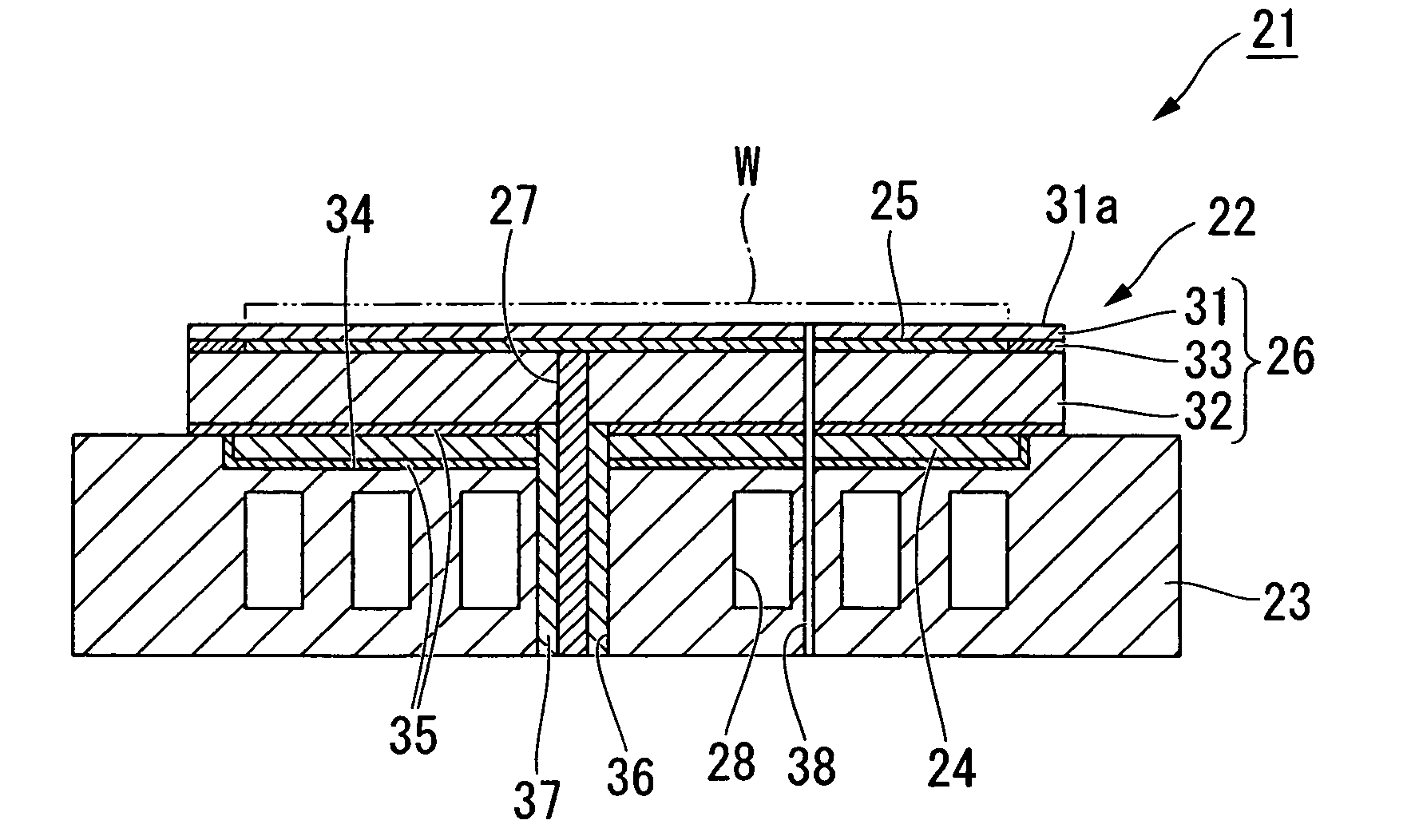
[0055]FIG. 1 is a cross-sectional view illustrating an electrostatic chuck device 21 according to a first embodiment of the invention. The electrostatic chuck device 21 includes an electrostatic chuck section 22, a metal base section 23, and a dielectric plate 24.

[0056]The electrostatic chuck section 22 includes a disc-like substrate 26, the top surface (one main surface) of which serves as a mounting surface for mounting a plate-like sample W and in which an electrostatic-adsorption inner electrode 25 is built, and a power supply terminal 27 for applying a DC voltage to the electrostatic-adsorption inner electrode 25.

[0057]The substrate 26 roughly...


PUM


Abstract

An electrostatic chuck device which enables to perform a plasma process having high in-plane uniformity to a plane-like sample by improving the in-plane uniformity of the electric field intensity in a plasma when applied to a plasma processing apparatus. Specifically disclosed is an electrostatic chuck device (21) including an electrostatic chuck section (22), a metal base section (23) serving as a high-frequency generating electrode, and an insulating plate (24). The electrostatic chuck section (22) is composed of a dielectric plate (31) whose top surface (31a) serves as a mounting surface on which a plate-like sample (W) is placed, a supporting plate (32), an electrostatic-adsorption inner electrode (25), and an insulating layer (33). The electrostatic-adsorption inner electrode (25) is made of a composite sintered body containing an insulating ceramic and silicon carbide, while having a volumetric resistance of not less than 1.0×10⁻¹ Ωcm but not more than 1.0×10⁸ Ωcm.

Description

[0001]This application is a National Stage Application of PCT / JP2007 / 065073, filed 1 Aug. 2007, which claims benefit of Serial No. 2006-218449, filed 10 Aug. 2006 in Japan and which application(s) are incorporated herein by reference. To the extent appropriate, a claim of priority is made to each of the above disclosed applications.BACKGROUND OF THE INVENTION[0002]1. Field of the Invention[0003]The present invention relates to an electrostatic chuck device, and more particularly, to an electrostatic chuck device suitable for use in a high-frequency discharge type plasma processing apparatus for applying a high-frequency voltage to an electrode to generate plasma and processing a plate-like sample such as a semiconductor wafer, a metal wafer, and a glass plate by the use of the generated plasma.[0004]2. Description of the Related Art[0005]Conventionally, plasma was often used in processes such as etching, deposition, oxidation, and sputtering for manufacturing semiconductor devices s...

Claims


Application Information

Patent Timeline
Patent Type & Authority Patents(United States)
IPC IPC(8): H02H1/00
CPCH01L21/6833H02N13/00Y10T279/23H01L21/3065H01L21/0262
Inventor INAZUMACHI, HIROSHIKOSAKAI, MAMORUMIURA, YUKIOMAKI, KEIGO
Owner SUMITOMO OSAKA CEMENT CO LTD
Why Eureka
Try Eureka