High-speed multi-type substrate analog to digital converter

Active Publication Date: 2012-10-02
CSR TECH INC
View PDF1 Cites 4 Cited by
  • Summary
  • Abstract
  • Description
  • Claims
  • Application Information

AI Technical Summary

Benefits of technology

[0006]High conversion rates are achieved in an analog to digital converter by tailoring the substrate type to specific operational elements of the converter. Embodiments place sample and hold processing circuitry on a substrate type having properties that allow for faster processing at high sampling / clock frequencies. Other operational elements of the converter are constructed on at least one other substrate type in keeping with the remainder of the circuitry for which the converter is being implemented. The sample and hold substrate may be implemented on any material which is capable of faster processing, such as silicon germanium, gallium arsenide, silicon bipolar, BiCMOS and the like. Other portions may be implemented on a more CMOS substrate. Such systems are counter to the current development trends of the art as implementation is split onto separate circuits. Further, such systems are able to implement analog-to digital conversion for broadband signals at high speeds without the need for extensive timing compensation, while also avoiding problems due to noise from further digital processing circuitry.
[0008]In more detailed embodiments, the tuner system may include a phase- locked loop (PLL) circuit on the first substrate which is configured to provide a sampling frequency signal to the sample and hold portion. This PLL circuit may be further configured to provide a clock signal to the conversion portion and digital signal processing circuitry. Embodiments may place various components on the differing substrates in accordance with performance capabilities of the respective substrates and to achieve noise isolation goals. For example, a PLL circuit may have improved jitter performance when implemented on a non-CMOS substrate. Additionally, it may be advantageous to isolate digital processing circuitry from sample and hold circuitry to mitigate noise errors.

Problems solved by technology

Such systems are counter to the current development trends of the art as implementation is split onto separate circuits.

Method used


Image

  • High-speed multi-type substrate analog to digital converter
  • High-speed multi-type substrate analog to digital converter
  • High-speed multi-type substrate analog to digital converter

Examples


Embodiment Construction

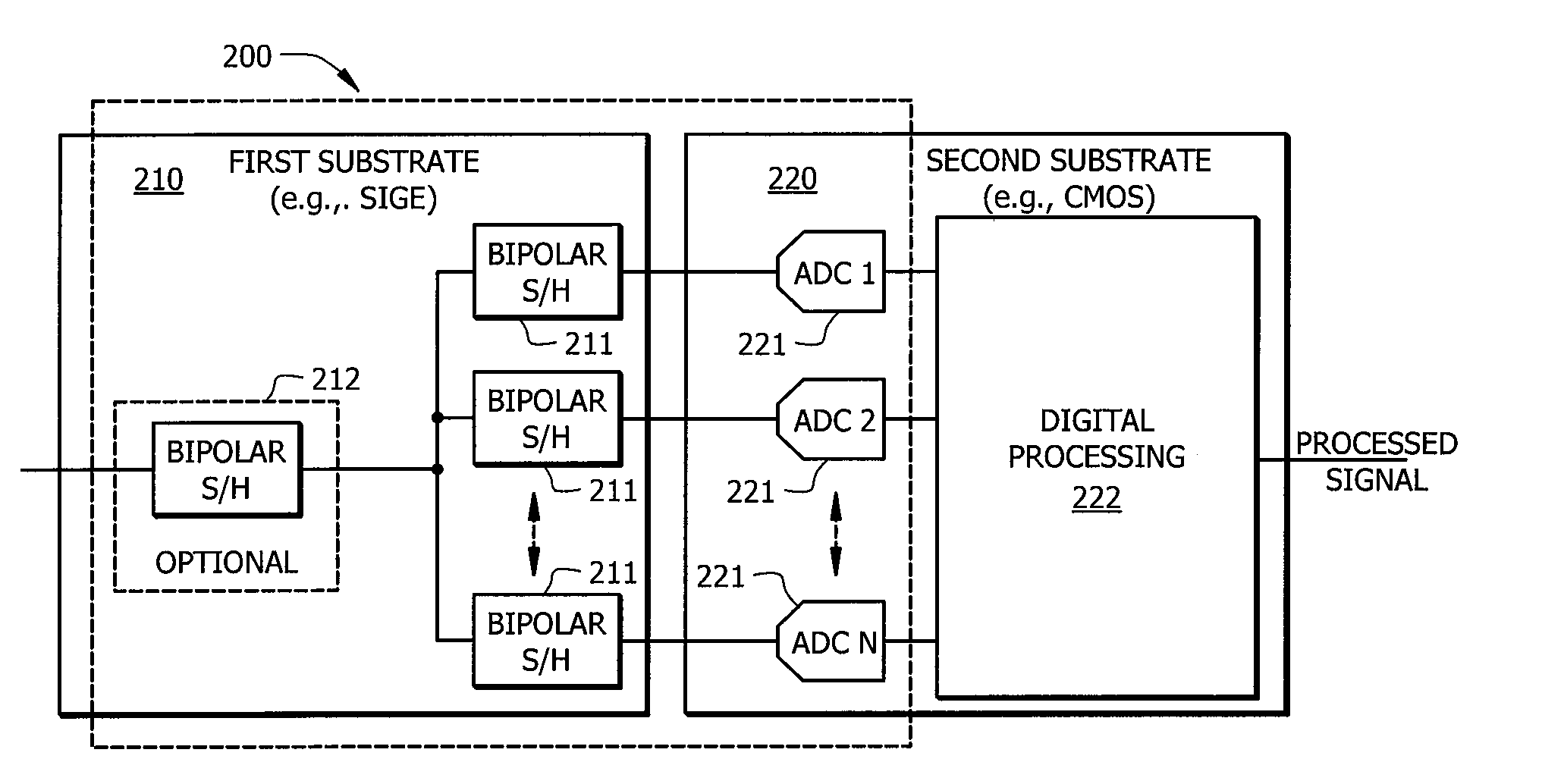
[0017]FIG. 2 illustrates an ADC architecture 200 in accordance with an embodiment of the present invention. In this embodiment, ADC architecture 200 is split between a first substrate 210 and a second substrate 220. First substrate 210 is manufactured from a material which is capable of better performance than a CMOS circuit at high frequencies. Examples of such materials are silicon germanium, gallium arsenide, silicon bipolar, BiCMOS and the like. Such better performance may include allowing for improved settling time of sample and hold circuitry at high sample rates. Additionally, such performance may include improved jitter control for sampling clock at high sampling rates. First substrate 210 includes sample and hold circuitry 211. In some embodiments sample and hold circuitry 211 is implemented as a bipolar sample and hold which utilizes at least one bipolar transistor. The use of a bipolar transistor offers advantages over standard sample and hold circuitry implemented in CMO...


PUM


Abstract

High conversion rates are achieved in an analog to digital converter by tailoring the substrate type to specific operational elements of the converter. Embodiments place sample and hold processing circuitry on a substrate type having properties that allow for faster processing at high sampling / clock frequencies. Other operational elements of the converter are constructed on at least one other substrate type in keeping with the remainder of the circuitry for which the converter is being implemented. The sample and hold substrate may be implemented on any material which is capable of faster processing, such as silicon germanium, gallium arsenide, silicon bipolar, BiCMOS, and the like. Other portions may be implemented on a more CMOS substrate. Such systems and methods are able to implement analog-to digital conversion for broadband signals at high speeds without the need for extensive timing compensation, while also avoiding problems due to noise from further digital processing circuitry.

Description

TECHNICAL FIELD[0001]The present disclosure relates generally to signal processing devices and analog-to-digital conversion of signals. More specifically, the present disclosure relates to improving performance of signal processing devices by splitting functionality of the devices between multiple substrate types.BACKGROUND[0002]In current tuner systems digital processing is generally implemented in complimentary metal-oxide-semiconductor (CMOS) only processes. Additionally, in the tuner industry, as with many industries, there is a general trend to miniaturize and compact all circuitry onto a single circuit which is capable of accomplishing a manufacturer's design and performance goals. Accordingly, current tuner systems and their corresponding digital processing needs are normally implemented within a single circuit (e.g. CMOS) framework. Moreover, when design issues occur, solutions to these problems are sought within this single circuit framework.[0003]Current analog-to-digital ...

Claims


Application Information

Patent Timeline
IPC IPC(8): H03M1/12
CPCH03M1/0827H03M1/1245
Inventor STEVENSON, JAN-MICHAEL
Owner CSR TECH INC
Why Eureka
Try Eureka