Phase locked loop circuitry having switched resistor loop filter circuitry, and methods of operating same

a filter circuit and phase lock technology, applied in the direction of pulse automatic control, electrical apparatus, network with variable switch closing time, etc., can solve the problems of affecting the noise sensitivity of the pll, affecting the goal of achieving low silicon area, and adding to the manufacturing cost of the intended product for the pll

Active Publication Date: 2012-10-30
SITIME
View PDF7 Cites 24 Cited by
  • Summary
  • Abstract
  • Description
  • Claims
  • Application Information

AI Technical Summary

Benefits of technology

[0003]While the existing analog and digital PLL structures are now well proven and can satisfy the performance needs for a wide variety of applications, they have shortcomings when trying to achieve complete integration of the PLL with low silicon area and low power consumption. On the analog side, charge pump PLLs are well known to require a very large capacitor in their loop filter, which directly impedes the goal of achieving low silicon area. In fact, it is not uncommon for the capacitor area requirements to be so large that it must be placed off-chip, which negatively impacts the noise sensitivity of the PLL and adds to manufacturing cost of the intended product for the PLL. In addition, 1 / f noise from the charge pump is often a significant issue when seeking low phase noise for the PLL. On the digital side, an advantage of the digital PLL is that its loop filter can be quite small in area and easily configured for a wide variety of applications, and a well designed TDC can achieve low 1 / f noise. However, since a digital PLL contains many signals that continuously switch between supply and ground, achieving very low power consumption can be challenging, especially if older CMOS fabrication processes, such as 0.18 u CMOS, are utilized.
[0007]3) phase detector architectures, topologies and circuitry that reduce the impact of loop filter noise by achieving high gain in their detection characteristic, and

Problems solved by technology

On the analog side, charge pump PLLs are well known to require a very large capacitor in their loop filter, which directly impedes the goal of achieving low silicon area.
In fact, it is not uncommon for the capacitor area requirements to be so large that it must be placed off-chip, which negatively impacts the noise sensitivity of the PLL and adds to manufacturing cost of the intended product for the PLL.
In addition, 1 / f noise from the charge pump is often a significant issue when seeking low phase noise for the PLL.
However, since a digital PLL contains many signals that continuously switch between supply and ground, achieving very low power consumption can be challenging, especially if older CMOS fabrication processes, such as 0.18 u CMOS, are utilized.

Method used


Image

  • Phase locked loop circuitry having switched resistor loop filter circuitry, and methods of operating same
  • Phase locked loop circuitry having switched resistor loop filter circuitry, and methods of operating same
  • Phase locked loop circuitry having switched resistor loop filter circuitry, and methods of operating same

Examples


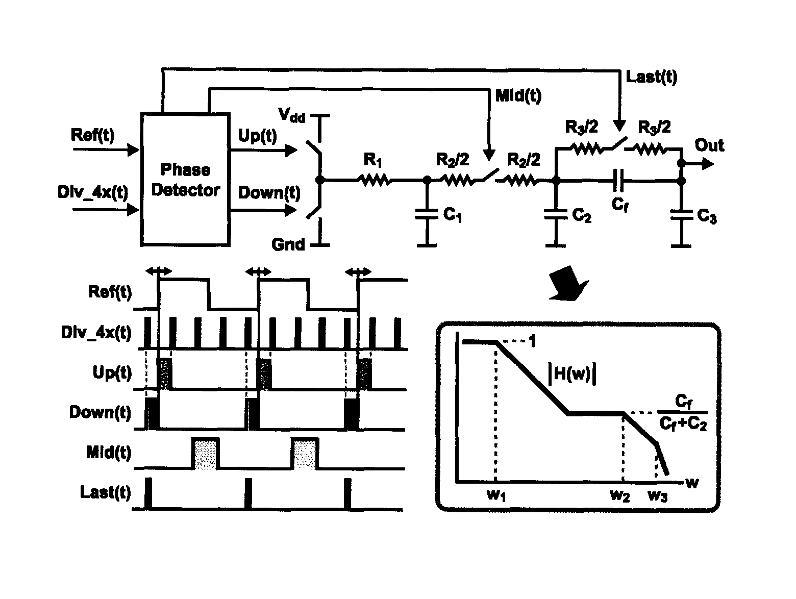
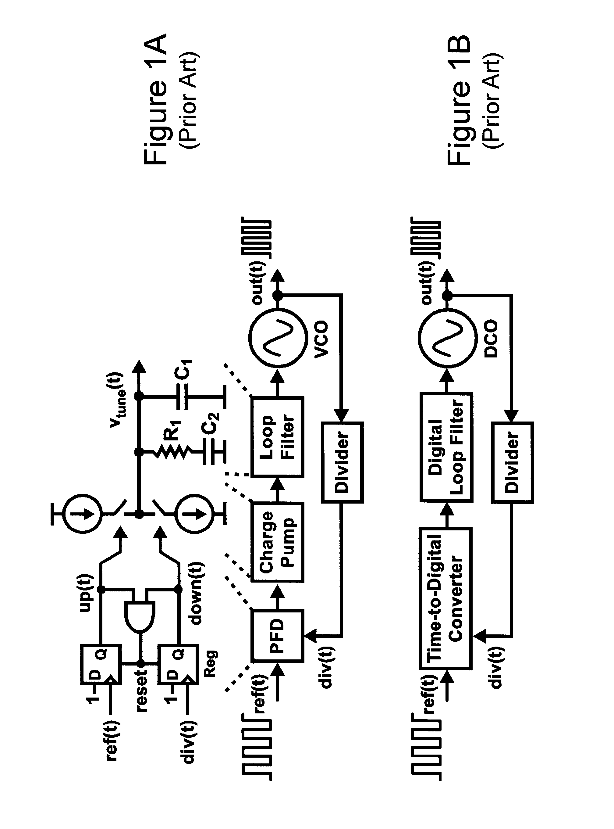
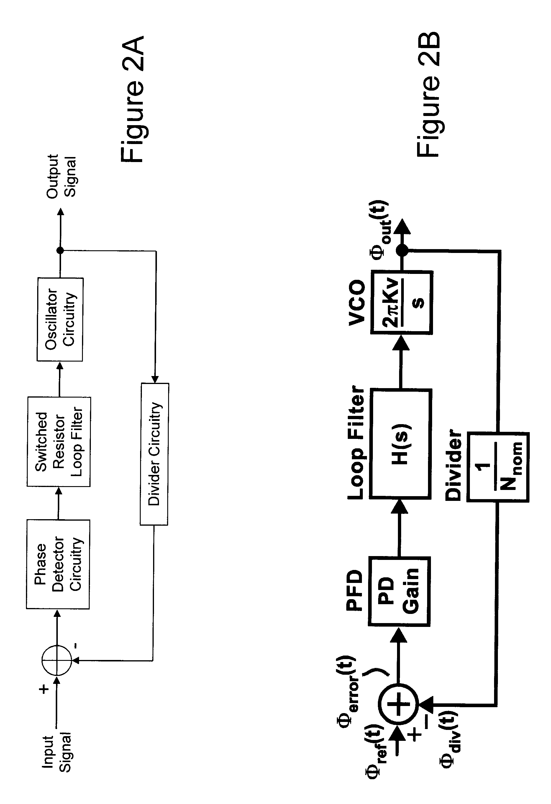
Embodiment Construction

[0064]At the outset, it should be noted that there are many inventions described and illustrated herein. The present inventions are neither limited to any single aspect nor embodiment thereof, nor to any combinations and / or permutations of such aspects and / or embodiments. Moreover, each of the aspects of the present inventions, and / or embodiments thereof, may be employed alone or in combination with one or more of the other aspects of the present inventions and / or embodiments thereof. For the sake of brevity, many of those permutations and combinations will not be discussed separately herein.

[0065]Further, in the course of describing and illustrating the present inventions, various structures, components, materials and / or elements, as well as combinations and / or permutations thereof, are set forth. It should be understood that structures, components, materials and / or elements other than those specifically described and illustrated, are contemplated and are within the scope of the pr...


PUM


Abstract

Phase-locked loop circuitry to generate an output signal, the phase-locked loop circuitry comprising oscillator circuitry, switched resistor loop filter, coupled to the input of the oscillator circuitry (which, in one embodiment, includes a voltage-controlled oscillator), including a switched resistor network including at least one resistor and at least one capacitor, wherein an effective resistance of the switched resistor network is responsive to and increases as a function of one or more pulsing properties of a control signal (wherein pulse width and frequency (or period) are pulsing properties of the control signal), phase detector circuitry, having an output which is coupled to the switched resistor loop filter, to generate the control signal (which may be periodic or non-periodic). The phase-locked loop circuitry may also include frequency detection circuitry to provide a lock condition of the phase-locked loop circuitry. The frequency detection circuitry includes (i) circuitry to generate a signal which is representative of the frequency of the output signal of the phase-locked loop circuitry, (ii) comparison circuitry to compare the signal which is representative of the frequency of the output signal of the phase-locked loop circuitry to a reference input to the phase-locked loop circuitry, and (iii) a switched capacitor network including at least one capacitor.

Description

RELATED APPLICATION[0001]This non-provisional application claims priority to U.S. Provisional Application Ser. No. 61 / 236,682, entitled “Switched Resistor Loop Filter Circuitry, Low Area / Power Implementation of Phase Locked Loop Circuits, and Methods of Manufacturing and Operating Same”, filed Aug. 25, 2009 (hereinafter “the Provisional Application”); the contents of the Provisional Application are incorporated by reference herein, in their entirety.INTRODUCTION[0002]Phase-locked loop (PLL) circuits are a key component of most modern communication circuits, and are also used in a variety of digital processor applications in order to generate high frequency, low jitter clock sources. While there are a wide variety of PLL architectures that have been proposed, the charge pump PLL, which is shown in FIG. 1A, has emerged as the most popular analog implementation, and is composed of a phase / frequency detector (PFD), charge pump, RC network, voltage controlled oscillator (VCO), and freque...

Claims


Application Information

Patent Timeline
Patent Type & Authority Patents(United States)
IPC IPC(8): H03L7/06
CPCH03H19/008H03L7/085H03L7/087H03L7/1976H03L7/093H03L7/113H03L7/183H03L7/091H03L7/0992H03L7/0802H03L7/089
Inventor PERROTT, MICHAEL H.
Owner SITIME
Why Eureka
Try Eureka