Methods of forming pattern structures

a pattern structure and pattern technology, applied in the field of pattern structure, can solve the problems of low etching rate of metal, difficult formation of hard masks for etching process having high etching selectivity, and inability to etch structures below hard masks to achieve desirable shapes, etc., to achieve the effect of suppressing the removal of mask patterns

Active Publication Date: 2012-12-18
SAMSUNG ELECTRONICS CO LTD
View PDF28 Cites 56 Cited by
  • Summary
  • Abstract
  • Description
  • Claims
  • Application Information

AI Technical Summary

Benefits of technology

[0009]Example embodiments relate to a method of manufacturing a memory device having good operational characteristics for reducing process defects.
[0025]According to example embodiments, a method of forming a patterned object layer includes forming an object layer on a substrate. The method may further include forming a mask pattern on the object layer, and performing an etching process using a mixed etching gas including at least ammonia gas and oxygen gas to form a patterned object layer. The oxygen gas may suppress the removal of the mask pattern during the etching process.
[0028]In example embodiments, the method may be used to manufacture a magnetic memory device, the method including forming a conductive pattern on a substrate, forming a lower magnetic layer, a tunnel barrier layer and an upper magnetic layer on the conductive pattern, forming a hard mask pattern on the upper magnetic layer. The method may include etching the upper magnetic layer, the tunnel barrier layer, and the lower magnetic layer by an etching process using a mixed etching gas including ammonia (NH3) gas, together with oxygen gas, and a fluorine-containing gas to form a Magnetic Tunnel Junction (MTJ). The oxygen gas may suppress the removal of the mask pattern during the etching process.

Problems solved by technology

The metal used in the memory devices may be patterned by a reactive etching process or a physical etching process; however, an etching rate for the metal may be very low.
Additionally, a hard mask for the etching process having a high etching selectivity may not be easily formed.
Specifically, the hard mask may be excessively removed during the etching process so that structures below the hard mask may not be patterned into a desirable shape.

Method used


Image

  • Methods of forming pattern structures
  • Methods of forming pattern structures
  • Methods of forming pattern structures

Examples


experiment 1

on Magnetoresistance Ratio

EXAMPLE 1

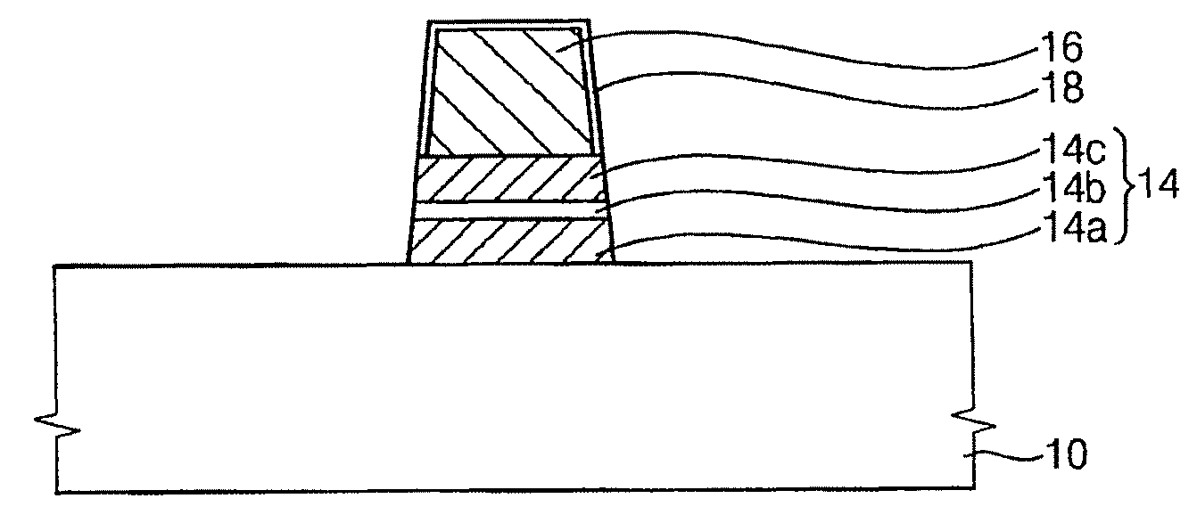
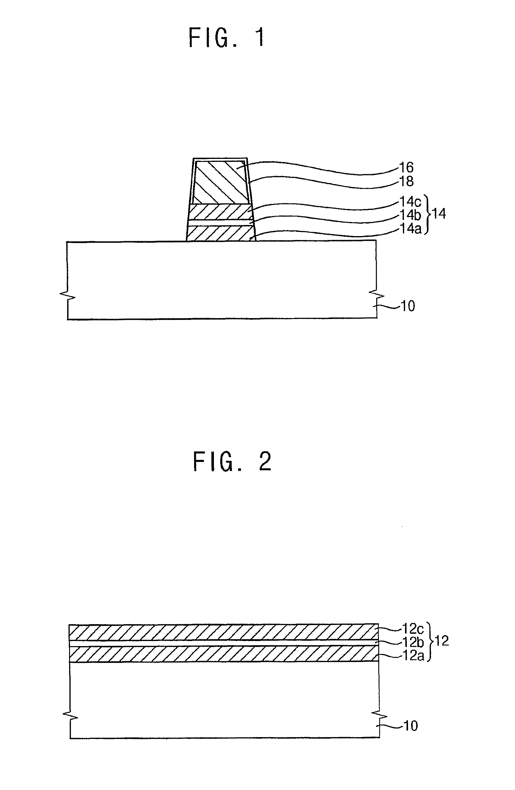
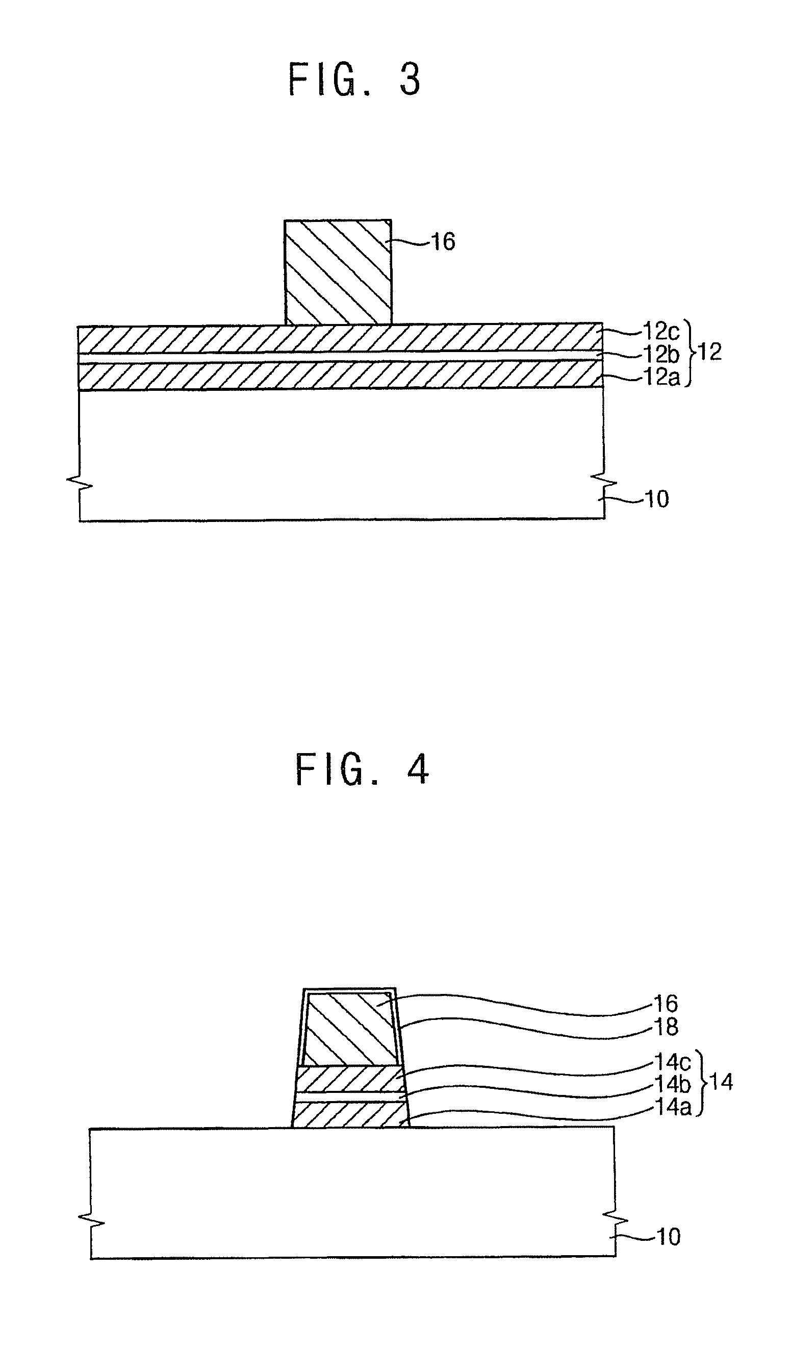
[0168]FIG. 17 is a cross-sectional view illustrating a MTJ structure in accordance with Example 1.

[0169]The MTJ structure was formed as follows.

[0170]Referring to FIG. 10, a MTJ material layer was formed on a substrate 10. Specifically, a first barrier layer was formed on the substrate 10 using tantalum (Ta). A fixed layer was formed on the first barrier layer using PtMn. A CoFe layer, a Ru layer and a CoFe layer were stacked sequentially on the fixed layer. A second barrier layer (i.e., a tunnel barrier layer) was formed on the CoFe layer using MgO. A free layer was formed on the tunnel barrier layer using CoFeB.

[0171]A hard mask layer including a titanium layer and titanium nitride layer. The hard mask layer was patterned to form a hard mask 16 including a titanium layer pattern and a titanium nitride layer pattern. The hard mask 16 was formed to have a line width of about 50 nm.

[0172]The MTJ material layer was etched using the hard mask as an et...


PUM


Abstract

An example embodiment relates to a method of forming a pattern structure, including forming an object layer on a substrate, and forming a hard mask on the object layer. A plasma reactive etching process is performed on the object layer using an etching gas including a fluorine containing gas and ammonia (NH3) gas together with oxygen gas to form a pattern. The oxygen gas is used for suppressing the removal of the hard mask during the etching process.

Description

CROSS-REFERENCE TO RELATED APPLICATIONS[0001]This application is a Continuation-In-Part Application claiming priority under 35 U.S.C. §120 of U.S. patent application Ser. No. 12 / 940,535, filed on Nov. 5, 2010 now U.S. Pat. No. 8,158,445, which claims priority under 35 U.S.C. §119 to Korean Patent Application Nos. 10-2009-0108712 and 10-2010-0004570, filed on Nov. 11, 2009 and Jan. 19, 2010, respectively, in the Korean Intellectual Property Office (KIPO). This application also claims priority under 35 U.S.C. §119 to the benefit of Korean Patent Application No. 10-2010-0069071, filed on Jul. 16, 2010, in the Korean Intellectual Property Office. The entire contents of each of the above-mentioned applications are incorporated herein by reference.BACKGROUND[0002]1. Field[0003]Example embodiments relate to pattern structures, methods of forming the same and methods of manufacturing semiconductor devices using the same. More particularly, example embodiments relate to pattern structures in...

Claims


Application Information

Patent Timeline
Patent Type & Authority Patents(United States)
IPC IPC(8): H01L21/00
CPCH01L27/228H01L43/12H10B61/22H10N50/01
Inventor JEONG, JUN-HOLEE, JANG-EUNKIM, WOO-JINSHIN, HEE-JURYU, YONG-HWAN
Owner SAMSUNG ELECTRONICS CO LTD
Why Eureka
Try Eureka