Semiconductor device and method of manufacturing same

a semiconductor and device technology, applied in the direction of semiconductor devices, electrical appliances, transistors, etc., can solve the problem of increasing the cost from the standpoint of the ratio relative to the performance, and achieve the effect of improving the performance of a semiconductor devi

Inactive Publication Date: 2012-12-25
RENESAS ELECTRONICS CORP
View PDF19 Cites 1 Cited by
  • Summary
  • Abstract
  • Description
  • Claims
  • Application Information

AI Technical Summary

Benefits of technology

[0017]As described above, the tensile stress film TSL101 is formed at the nMIS region 101A, and the compression stress film CSL101 is formed at the pMIS region 101B. The application of the tensile stress by the tensile stress film TSL101 at the channel region of the n-channel type MISFET formed at the nMIS region 101A can improve the mobility in the channel region, and the application of the compression stress of the compression stress film CSL101 to the channel region of the p-channel type MISFET formed at the pMIS region 101B can improve the mobility in the channel region. This can improve ON current of both n-channel type MISFET and p-channel type MISFET.
[0019]That is, it was found that, upon dry-etching the stress film (the tensile stress film TSL101 in the case of FIG. 111) in the process of FIG. 111, the metal silicide layer 113 may be over-etched to generate the decrease in the thickness or etching damage of the metal silicide layer 113, to raise the resistance of the metal silicide layer 113. Since the metal silicide layer 113 is provided for lowering the resistance, a lower resistance of the metal silicide layer 113 is desirable, and the increase in the resistance of the metal silicide layer 113 may lower the performance of the semiconductor device. The problem of the rise in the resistance of the metal silicide layer 113 caused by the over etching of the metal silicide layer 113 may occur in both cases where the stress film to be etched in the process in FIG. 111 is the tensile stress film or the compression stress film.
[0020]A target of the present invention is to provide a technology capable of improving the performance of semiconductor devices.
[0030]According to the representative embodiment, the performance of a semiconductor device can be improved.

Problems solved by technology

However, the improvement of the performance of transistor only by the miniaturization leads to such problem as the rise in the cost from the standpoint of the ratio relative to the performance.

Method used


Image

  • Semiconductor device and method of manufacturing same
  • Semiconductor device and method of manufacturing same
  • Semiconductor device and method of manufacturing same

Examples


embodiment 1

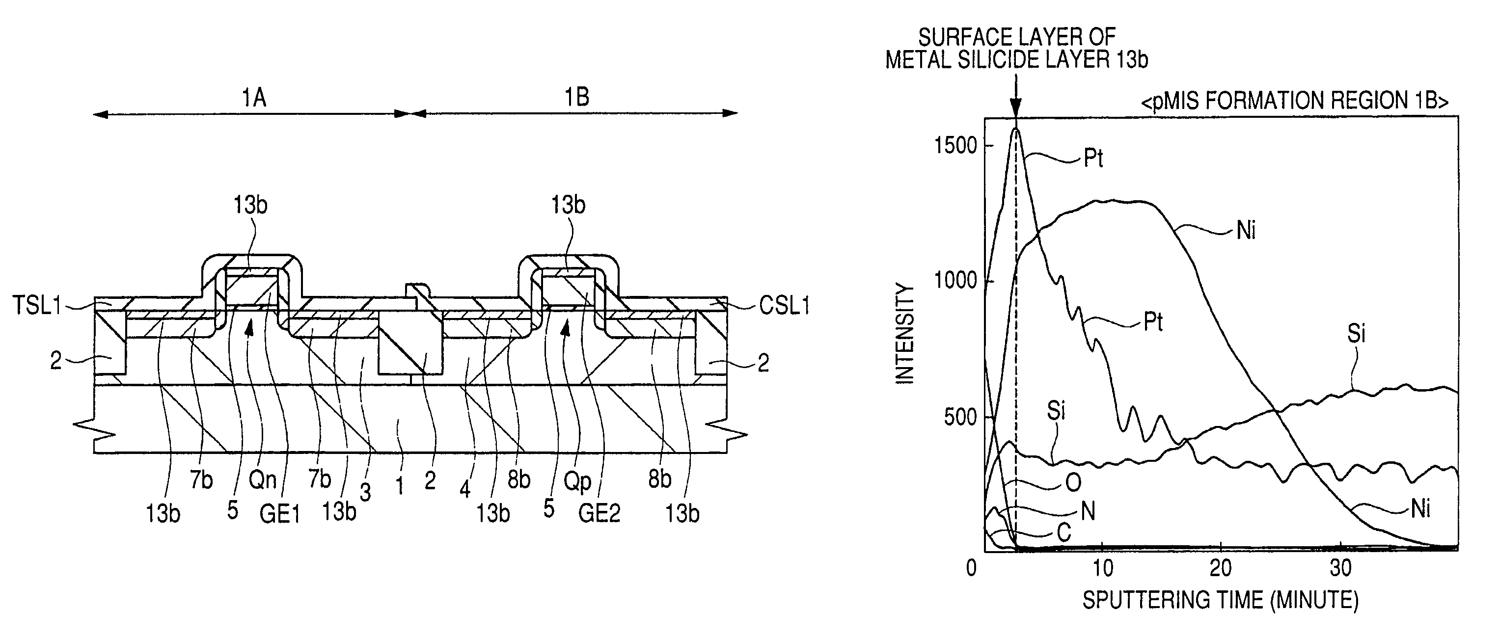
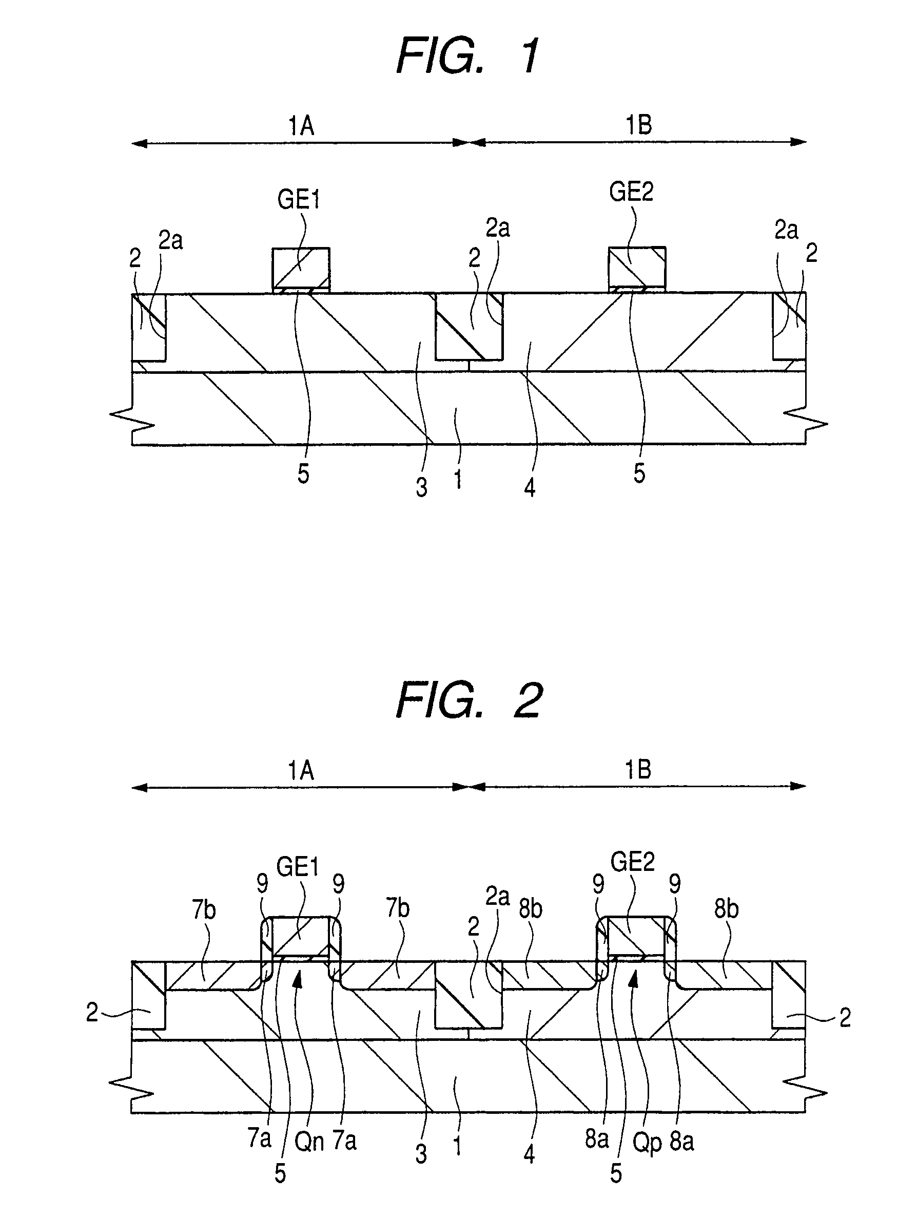
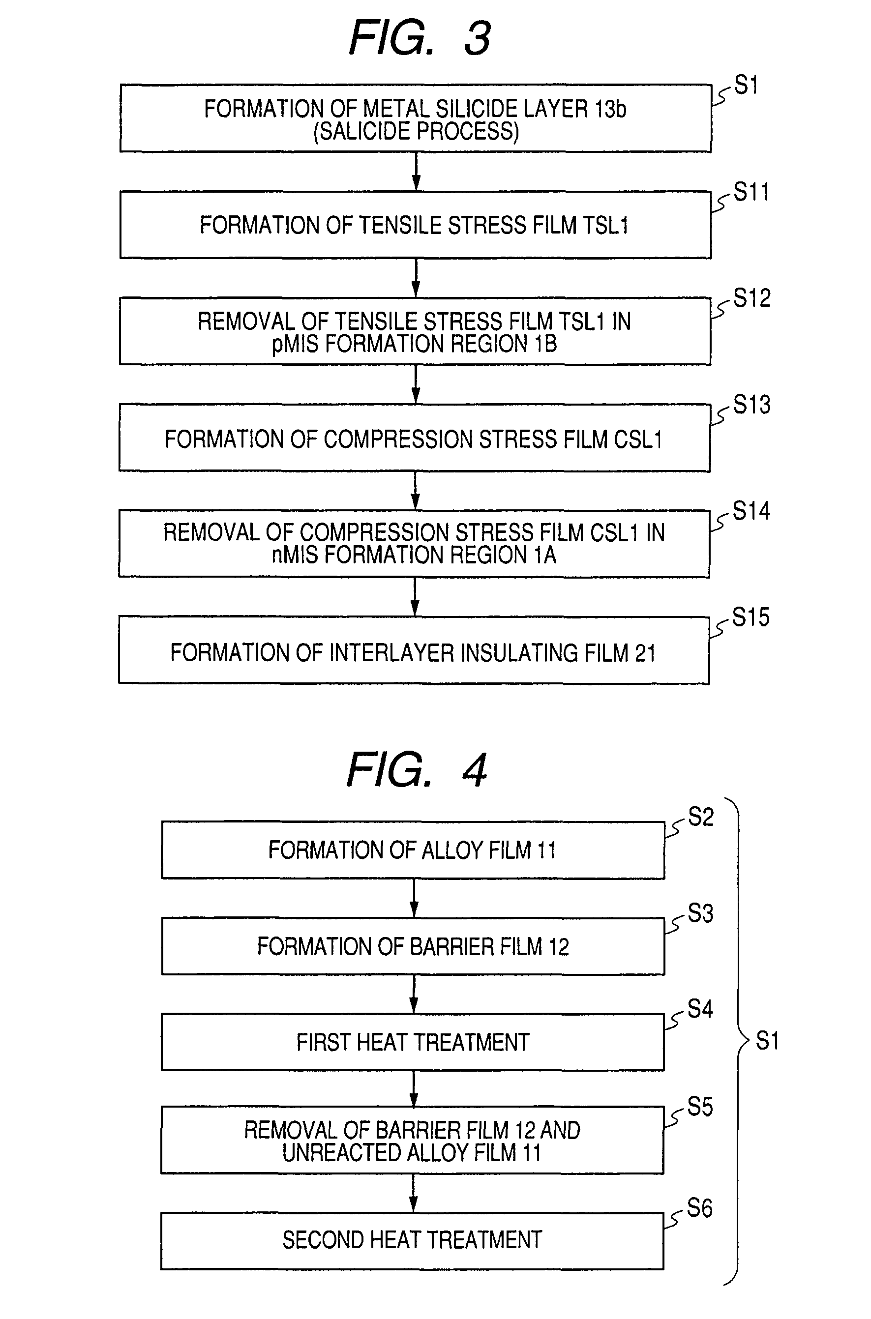
[0148]A manufacturing process of a semiconductor device of the embodiment will be described referring to drawings. FIGS. 1 and 2 are cross-sectional views of the essential part in a manufacturing process of the semiconductor device, here, the semiconductor device having a CMISFET (Complementary Metal Insulator Semiconductor Field Effect Transistor) being one embodiment of the invention.

[0149]Firstly, as shown in FIG. 1, a semiconductor substrate (a semiconductor wafer) 1 made of a p-type single crystalline silicon having a specific resistance of, for example, around 1 to 10 Ωcm, or the like, is prepared. The semiconductor substrate 1 at which a semiconductor device of the embodiment is formed has an nMIS formation region 1A being a region in which an n-channel type MISFET (Metal Insulator Semiconductor Field Effect Transistor) is to be formed, and a pMIS formation region 1B being a region in which a p-channel type MISFET is to be formed. Then, at the main face of the semiconductor s...

embodiment 2

[0217]FIG. 21 is a manufacturing process flow chart showing a part of the manufacturing process of a semiconductor device of the present embodiment, which corresponds to FIG. 3 in Embodiment 1. FIG. 22 is a cross-sectional view of the essential part in a manufacturing process of a semiconductor device of the embodiment, which shows the neighborhood of the metal silicide layer 13b of the nMIS formation region 1A and pMIS formation region 1B.

[0218]The embodiment corresponds to a first modification of Embodiment 1. The manufacturing process of a semiconductor device of the embodiment is the same as that in Embodiment 1 up to the formation of the metal silicide layer 13b at Step S1, and the description thereof is omitted here.

[0219]In the embodiment, after the formation of the metal silicide layer 13b at Step Si above (that is, after the second heat treatment at Step S6 above), the surface of the metal silicide layer 13b is oxidized (Step S21 in FIG. 21). The oxidation process at Step S...

embodiment 3

[0226]FIG. 23 is a manufacturing process flow chart showing a part of the manufacturing process of a semiconductor device of the present embodiment, which corresponds to FIG. 3 in Embodiment 1. FIGS. 24 to 28 are cross-sectional views of the essential part in a manufacturing process of a semiconductor device of the embodiment.

[0227]The embodiment corresponds to a second modification of Embodiment 1. The manufacturing process of a semiconductor device in the embodiment is the same as that in Embodiment 1 up to the formation of the tensile stress film TSL1 at Step S11 (that is, up to the obtainment of the structure in FIG. 8), and the description thereof is omitted here. Further, also in the embodiment, an oxidizing process of the surface of the metal silicide layer 13b at Step S21 may be added between the salicide process at Step S1 and the process for forming the tensile stress film TSL1 at Step S11, as in Embodiment 2.

[0228]In the embodiment, after the formation of the tensile stre...


PUM


Abstract

To improve the performance of semiconductor devices. Over an n+-type semiconductor region for source / drain of an n-channel type MISFET and a first gate electrode, and over a p+-type semiconductor region for source / drain of a p-channel type MISFET and a second gate electrode, which are formed over a semiconductor substrate, a metal silicide layer including nickel platinum silicide is formed by a salicide process. After that, a tensile stress film is formed over the whole face of the semiconductor substrate, and then the tensile stress film over the p-channel type MISFET is removed by dry-etching, and, after a compression stress film is formed over the whole face of the semiconductor substrate, the compression stress film over the n-channel type MISFET is removed by dry-etching. The Pt concentration in the metal silicide layer is highest at the surface, and becomes lower as the depth from the surface increases.

Description

CROSS-REFERENCE TO RELATED APPLICATION[0001]The disclosure of Japanese Patent Application No. 2009-55905 filed on Mar. 10, 2009 including the specification, drawings and abstract is incorporated herein by reference in its entirety.BACKGROUND OF THE INVENTION[0002]The present invention relates to a semiconductor device and a method of manufacturing the same, and, particularly, to a technology that is effective when applied to a semiconductor device that has a CMISFET and uses two stress films having different stress directions, and to the manufacture of the same.[0003]Presently, it is widely performed at miniaturize transistors and improve the performance thereof. However, the improvement of the performance of transistor only by the miniaturization leads to such problem as the rise in the cost from the standpoint of the ratio relative to the performance.[0004]Accordingly, a method has appeared which improves the performance of transistors by not only the miniaturization but also the ...

Claims


Application Information

Patent Timeline
Patent Type & Authority Patents(United States)
IPC IPC(8): H01L27/092H01L21/8238
CPCH01L21/823807H01L21/823814H01L21/823835H01L29/7843
Inventor YAMAGUCHI, TADASHITSUTSUMI, TOSHIAKIOGINO, SATOSHIYONEKURA, KAZUMASAKAWAI, KENJIMIYAGAWA, YOSHIHIROOKUDAIRA, TOMONORIKASHIHARA, KEIICHIROKIHARA, KOTARO
Owner RENESAS ELECTRONICS CORP
Why Eureka
Try Eureka