Semiconductor device and method for manufacturing the same

a semiconductor and semiconductor technology, applied in the field of semiconductor devices, can solve the problems of significant resistance increase, display unevenness, signal delay due to wiring resistance, etc., and achieve the effects of low parasitic capacitance, high on/off ratio, and high electric characteristics

Active Publication Date: 2012-12-25
SEMICON ENERGY LAB CO LTD
View PDF144 Cites 32 Cited by
  • Summary
  • Abstract
  • Description
  • Claims
  • Application Information

AI Technical Summary

Benefits of technology

[0009]For a thin film transistor in which an oxide semiconductor is used for a channel formation region, high speed operation, a comparatively easy manufacturing process, and sufficient reliability are required.
[0011]It is an object of an embodiment of the present invention to provide a semiconductor device in which the contact resistance between an oxide semiconductor layer used for a channel formation region and a source and drain electrodes is reduced, and to provide a method for manufacturing the semiconductor device.
[0015]Then, an oxide semiconductor layer containing indium, gallium, and zinc is used for a channel formation region, and buffer layers including an oxynitride containing indium, gallium, and zinc are interposed between the oxide semiconductor layer and a source and drain electrodes, whereby the contact resistance of a thin film transistor can be reduced.
[0024]According to an embodiment of the present invention, a thin film transistor with small parasitic capacitance and a high on / off ratio can be obtained. Accordingly, a semiconductor device with high electric characteristics and high reliability can be provided.

Problems solved by technology

In particular, when a display device with a large-area display is manufactured, a problem of signal delay due to the resistance of a wiring significantly arises.
However, in a thin film transistor having a structure in which an oxide semiconductor layer is in direct contact with a source and drain electrodes formed using a metal material, there is a concern that contact resistance increases.
For example, in a liquid crystal display device or a display device using an organic light-emitting element, there is a concern that display unevenness is caused due to variation in the transistor characteristics of the semiconductor device.
In particular, in a display device including a light-emitting element, in the case where there is a large variation in ON current (Ion) of TFTs (TFTs supplying current to a driver circuit or light-emitting elements arranged in pixels) arranged so as to supply a constant current to a pixel electrode, there is a concern that variation in the emission luminance of the light-emitting elements provided in the pixels is caused.

Method used


Image

  • Semiconductor device and method for manufacturing the same
  • Semiconductor device and method for manufacturing the same
  • Semiconductor device and method for manufacturing the same

Examples


embodiment 1

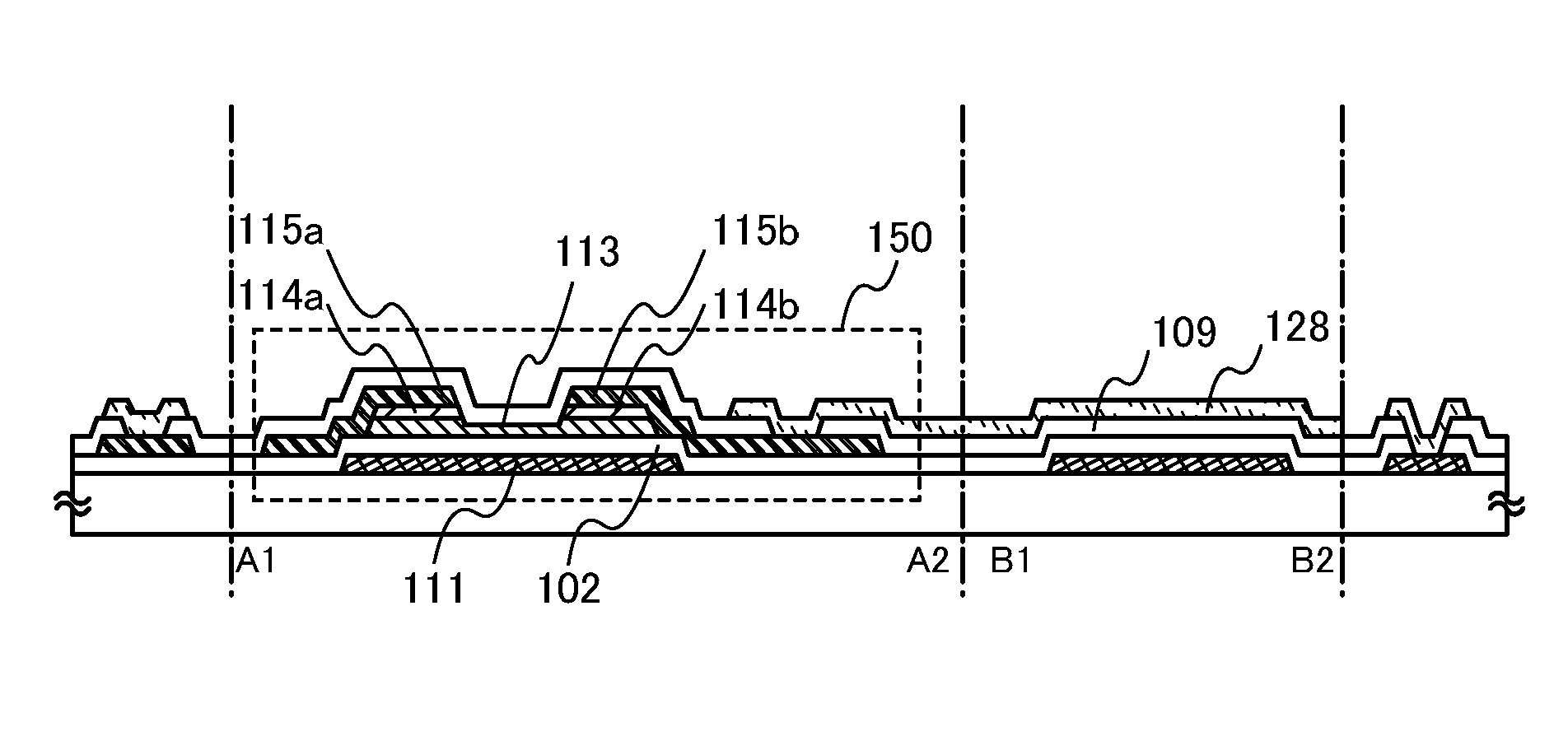
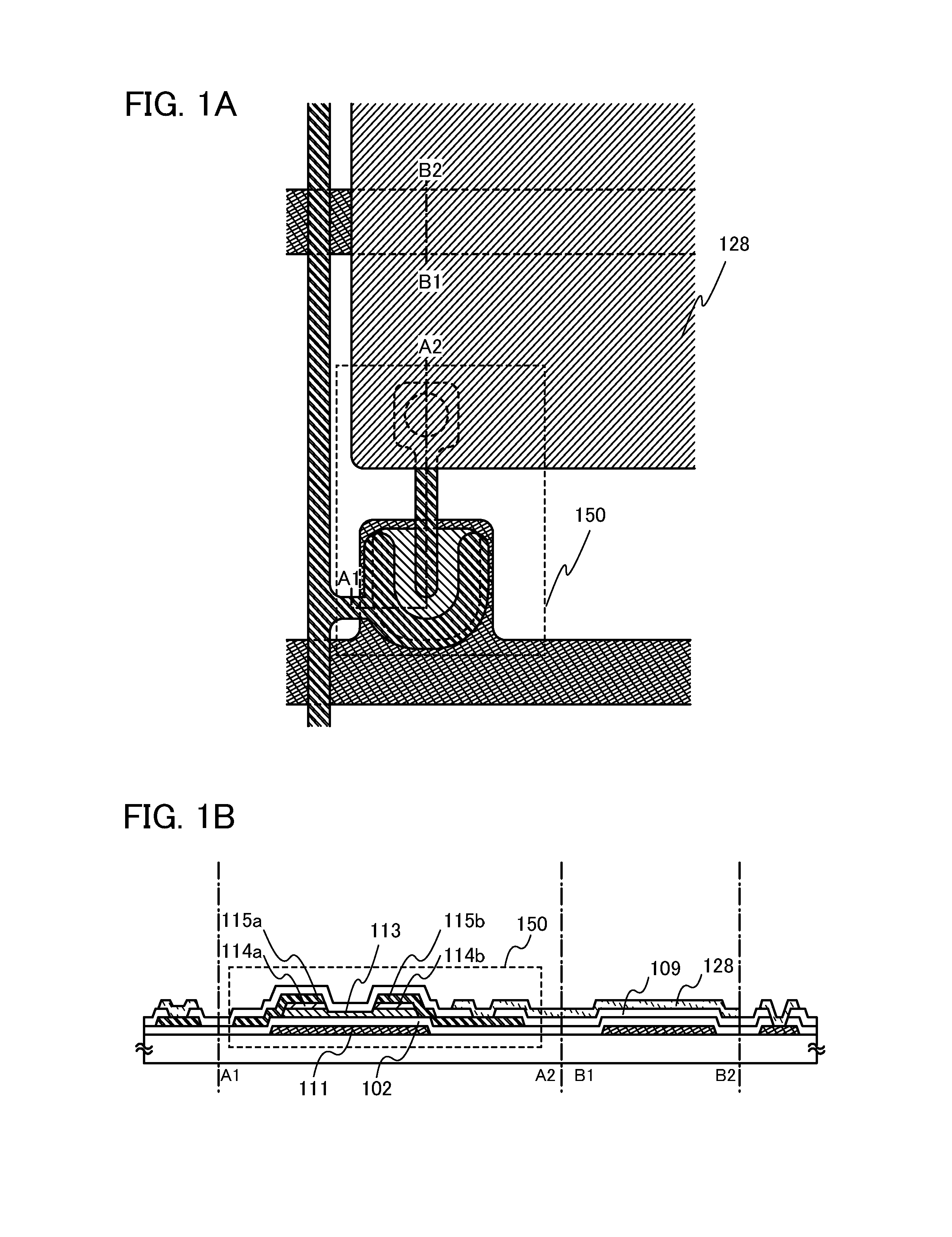
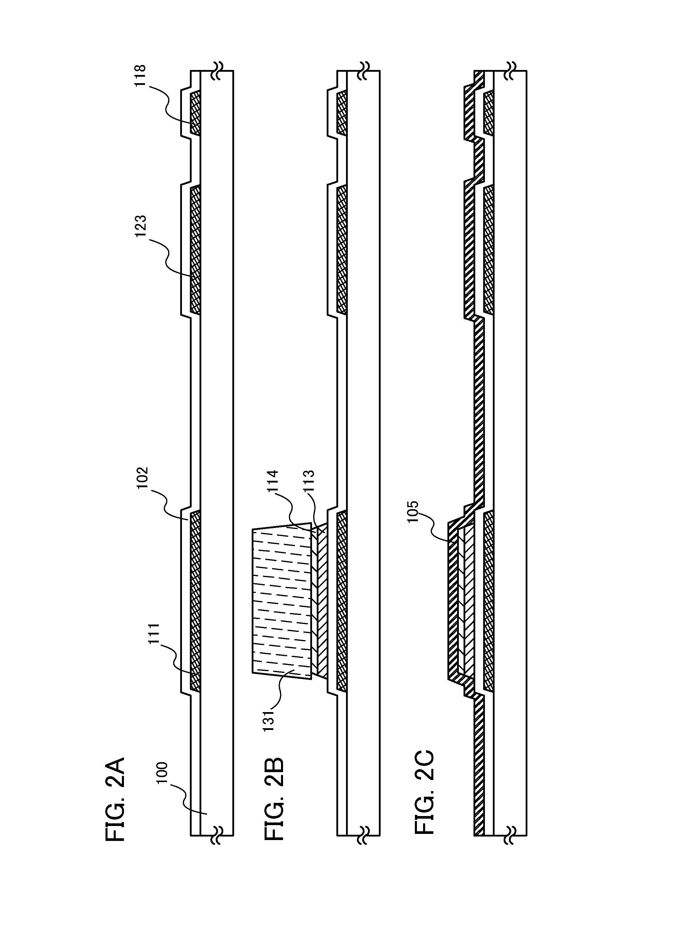
[0053]In this embodiment, a thin film transistor of a semiconductor device and a manufacturing process thereof will be described. Specifically, a manufacturing process of a pixel portion of a display device including a thin film transistor will be described.

[0054]FIGS. 1A and 1B illustrate a thin film transistor of this embodiment. FIG. 1A is a top view and FIG. 1B is a cross-sectional view taken along line A1-A2 and line B1-B2 of FIG. 1A.

[0055]An oxide semiconductor layer 113 of a thin film transistor 150 illustrated in FIGS. 1A and 1B is provided under a first electrode 115a and a second electrode 115b which face with each other, thereby covering a gate electrode 111 with a gate insulating film interposed therebetween. That is, the oxide semiconductor layer 113 is provided so as to overlap with the gate electrode 111 and be in contact with a top surface of the gate insulating film 102 and bottom surfaces of buffer layers (114a and 114b). Here, the buffer layer 114a is provided bet...

embodiment 2

[0099]In this embodiment, a thin film transistor of a semiconductor device and a manufacturing process thereof will be described. Specifically, a manufacturing process of a pixel portion of a display device including a thin film transistor will be described.

[0100]FIGS. 4A and 4B illustrate a thin film transistor of this embodiment. FIG. 4A is a plan view and FIG. 4B is a cross-sectional view taken along line A1-A2 and line B1 and B2 of FIG. 4A.

[0101]In a thin film transistor 151 illustrated in FIGS. 4A and 4B, a gate electrode 111 is formed over a substrate 100; a gate insulating film 102 is formed over the gate electrode 111; a first electrode 115a and a second electrode 115b which are to be a source and drain electrodes are formed over the gate insulating film 102 so that an end portion of the first electrode 115a and an end portion of the second electrode 115b overlap with the gate electrode 111. The oxide semiconductor layer 113 is provided so as to overlap with the gate electro...

embodiment 3

[0126]Here, an example in which an inverter circuit is formed using two n-channel thin film transistors which are formed in a manner similar to that of Embodiment 2 will be described below as an embodiment of the present invention.

[0127]A driver circuit for driving a pixel portion is formed using an inverter circuit, a capacitor, a resistor, and the like. When two n-channel TFTs are combined to form an inverter circuit, there are two types of combinations: a combination of an enhancement type transistor and a depletion type transistor (hereinafter, a circuit formed by such a combination is referred to as an “EDMOS circuit”) and a combination of enhancement type TFTs (hereinafter, a circuit formed by such a combination is referred to as an “EEMOS circuit”). Note that when the threshold voltage of the n-channel TFT is positive, the n-channel TFT is defined as an enhancement type transistor, while when the threshold voltage of the n-channel TFT is negative, the n-channel TFT is defined...


PUM

PropertyMeasurementUnit
strain pointaaaaaaaaaa
temperatureaaaaaaaaaa
sizesaaaaaaaaaa

Abstract

In a thin film transistor which uses an oxide semiconductor, buffer layers containing indium, gallium, zinc, oxygen, and nitrogen are provided between the oxide semiconductor layer and the source and drain electrode layers.

Description

BACKGROUND OF THE INVENTION[0001]1. Field of the Invention[0002]The present invention relates to a semiconductor device in which an oxide semiconductor film is used for a channel formation region, and a method for manufacturing the semiconductor device. For example, the present invention relates to thin film transistors, or electronic devices which are mounted with, as a component, electro-optical devices typified by liquid crystal display panels including a thin film transistor or electronic devices which have light-emitting display devices including an organic light-emitting element.[0003]In this specification, a “semiconductor device” refers to a device which can function by utilizing semiconductor characteristics; an electro-optical device, and an electronic device using a semiconductor circuit and a semiconductor element are all included in semiconductor devices.[0004]2. Description of the Related Art[0005]In recent years, active matrix display devices (such as liquid crystal d...

Claims


Application Information

Patent Timeline
Patent Type & Authority Patents(United States)
IPC IPC(8): H01L29/10H05B44/00
CPCH01L29/66742H01L29/78618H01L29/66969C04B35/58H01L29/7869H01L27/1225C04B2235/3284C04B2235/3286H01L29/78606H01L29/45
Inventor YAMAZAKI, SHUNPEISAKATA, JUNICHIROMARUYAMA, TETSUNORIIMOTO, YUKIASANO, YUJIKOEZUKA, JUNICHI
Owner SEMICON ENERGY LAB CO LTD
Why Eureka
Try Eureka