Flowable dielectric equipment and processes

a dielectric equipment and flow-through technology, applied in the field of manufacturing technology, can solve the problems of reducing the yield of reflow products, reducing the efficiency of reflow processes, so as to reduce the hydrogen, carbon and fluorine content of films, reduce the effect of undesirable components and reducing the contraction

Active Publication Date: 2013-01-22
APPLIED MATERIALS INC
View PDF368 Cites 154 Cited by
  • Summary
  • Abstract
  • Description
  • Claims
  • Application Information

AI Technical Summary

Benefits of technology

[0015]Embodiments may also include introducing a treatment gas such as oxygen (O2), ozone (O3), N2O, NO, NO2, NxHy including N2H4, H2, N2, NH3, and water vapor. The treatment gas may be introduced from the top of the processing chamber and excited in the first plasma region. Alternatively, the gas may be excited by a remote plasma before entering the first plasma region. This gas does not contribute appreciably to the film growth, but may be used to reduce hydrogen, carbon and fluorine content of the film while it is being grown or following growth. Hydrogen and nitrogen radicals induce a reduction in undesirable components of the growing film. Excited derivatives of the treatment gas assist the film by scavenging carbon and other atoms from the growing lattice, thereby reducing the contraction exhibited during the cure and the film stress present afterward.

Problems solved by technology

Some very narrow gaps, however, have continued to develop voids due, in part, to the lack of mobility following initial impact.
Reflowing the material after deposition can fill the void but, if the dielectric has a high reflow temperature (like SiO2), the reflow process may also consume a non-negligible portion of a wafer's thermal budget.
Unfortunately, low viscosity materials may shrink significantly during cure.
Significant film shrinkage results in high film stress and delamination issues, especially for thick films.
Growing films this way limits the time available for adsorbed species to remain mobile, a constraint which may result in deposition of nonuniform films.

Method used


Image

  • Flowable dielectric equipment and processes
  • Flowable dielectric equipment and processes
  • Flowable dielectric equipment and processes

Examples


Embodiment Construction

[0037]Disclosed embodiments include substrate processing systems that have a processing chamber and a substrate support assembly at least partially disposed within the chamber. At least two gases (or two combinations of gases) are delivered to the substrate processing chamber by different paths. A process gas can be delivered into the processing chamber, excited in a plasma, and pass through a showerhead into a second plasma region where it interacts with a silicon-containing gas and forms a film on the surface of a substrate. A plasma can be ignited in either the first plasma region or the second plasma region.

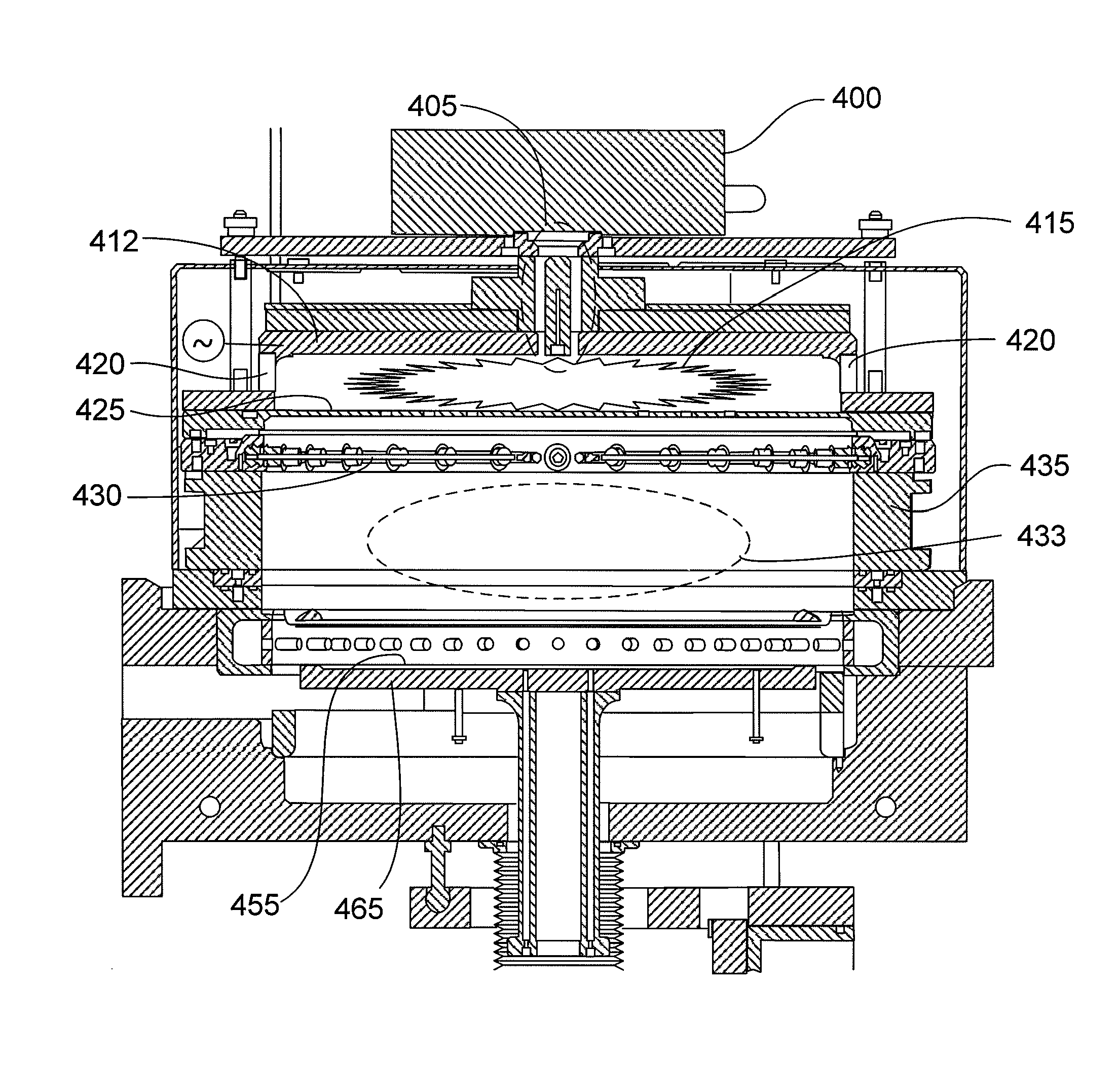
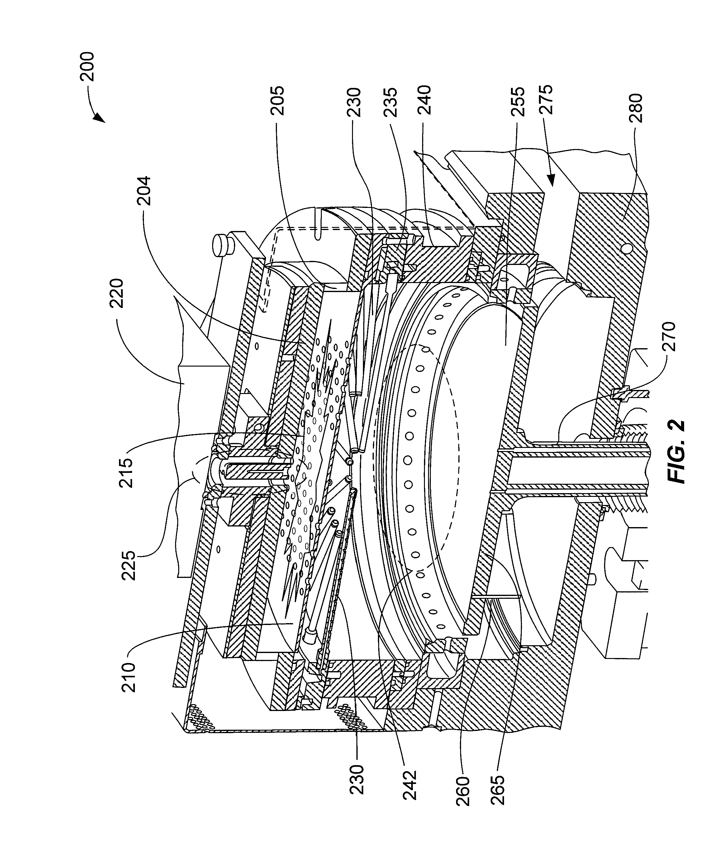
[0038]FIG. 2 is a perspective view of a process chamber with partitioned plasma generation regions which maintain a separation between multiple gas precursors. A process gas containing oxygen, hydrogen and / or nitrogen (e.g. oxygen (O2), ozone (O3), N2O, NO, NO2, NH3, NxHy including N2H4, silane, disilane, TSA, DSA, . . . ) may be introduced through the gas inlet assembly 225 ...


PUM

PropertyMeasurementUnit
diameteraaaaaaaaaa
diameteraaaaaaaaaa
diameteraaaaaaaaaa

Abstract

Methods of depositing and curing a dielectric material on a substrate are described. The methods may include the steps of providing a processing chamber partitioned into a first plasma region and a second plasma region, and delivering the substrate to the processing chamber, where the substrate occupies a portion of the second plasma region. The methods may further include forming a first plasma in the first plasma region, where the first plasma does not directly contact with the substrate, and depositing the dielectric material on the substrate to form a dielectric layer. One or more reactants excited by the first plasma are used in the deposition of the dielectric material. The methods may additional include curing the dielectric layer by forming a second plasma in the second plasma region, where one or more carbon-containing species is removed from the dielectric layer.

Description

CROSS-REFERENCES TO RELATED APPLICATIONS[0001]This application claims the benefit of U.S. Provisional Patent Application No. 61 / 052,080 field May 9, 2008. This application is also related to U.S. patent application Ser. No. 11 / 754,858, filed May 29, 2007, and titled “PROCESS CHAMBER FOR DIELECTRIC GAPFILL.” The entire contents of both applications are herein incorporated by reference for all purposes.FIELD[0002]This application relates to manufacturing technology solutions involving equipment, processes, and materials used in the deposition, patterning, and treatment of thin-films and coatings, with representative examples including (but not limited to) applications involving: semiconductor and dielectric materials and devices, silicon-based wafers and flat panel displays (such as TFTs).BACKGROUND[0003]A conventional semiconductor processing system contains one or more processing chambers and a means for moving a substrate between them. A substrate may be transferred between chamber...

Claims


Application Information

Patent Timeline
Patent Type & Authority Patents(United States)
IPC IPC(8): H05H1/24C23C16/00
CPCB08B7/00C23C16/4405C23C16/452C23C16/45514C23C16/509H01J37/32449
Inventor LUBOMIRSKY, DMITRYLIANG, QIWEIYANG, JANG GYOO
Owner APPLIED MATERIALS INC
Why Eureka
Try Eureka