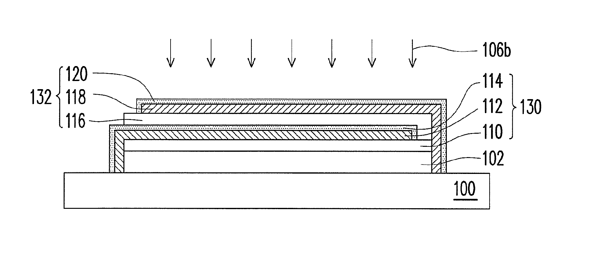
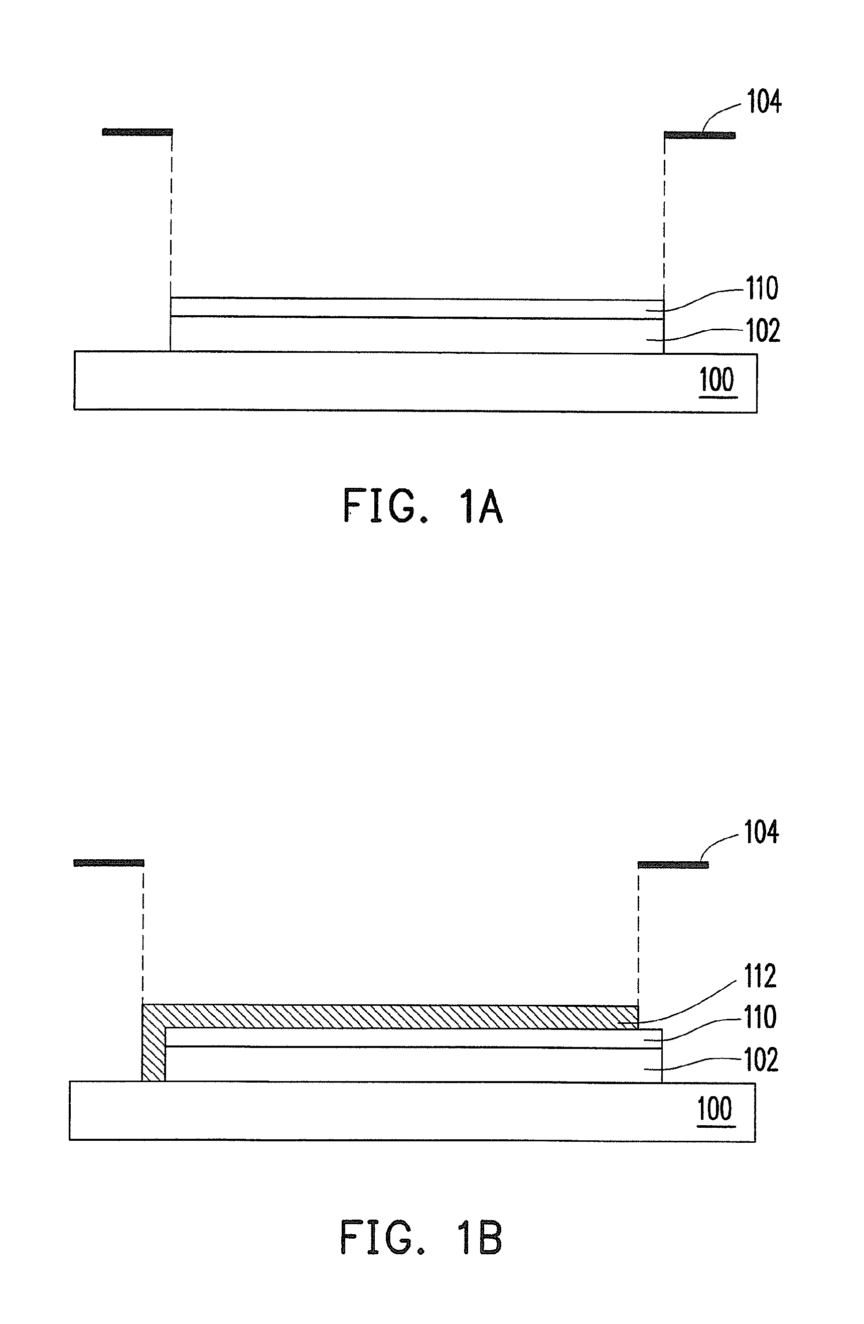
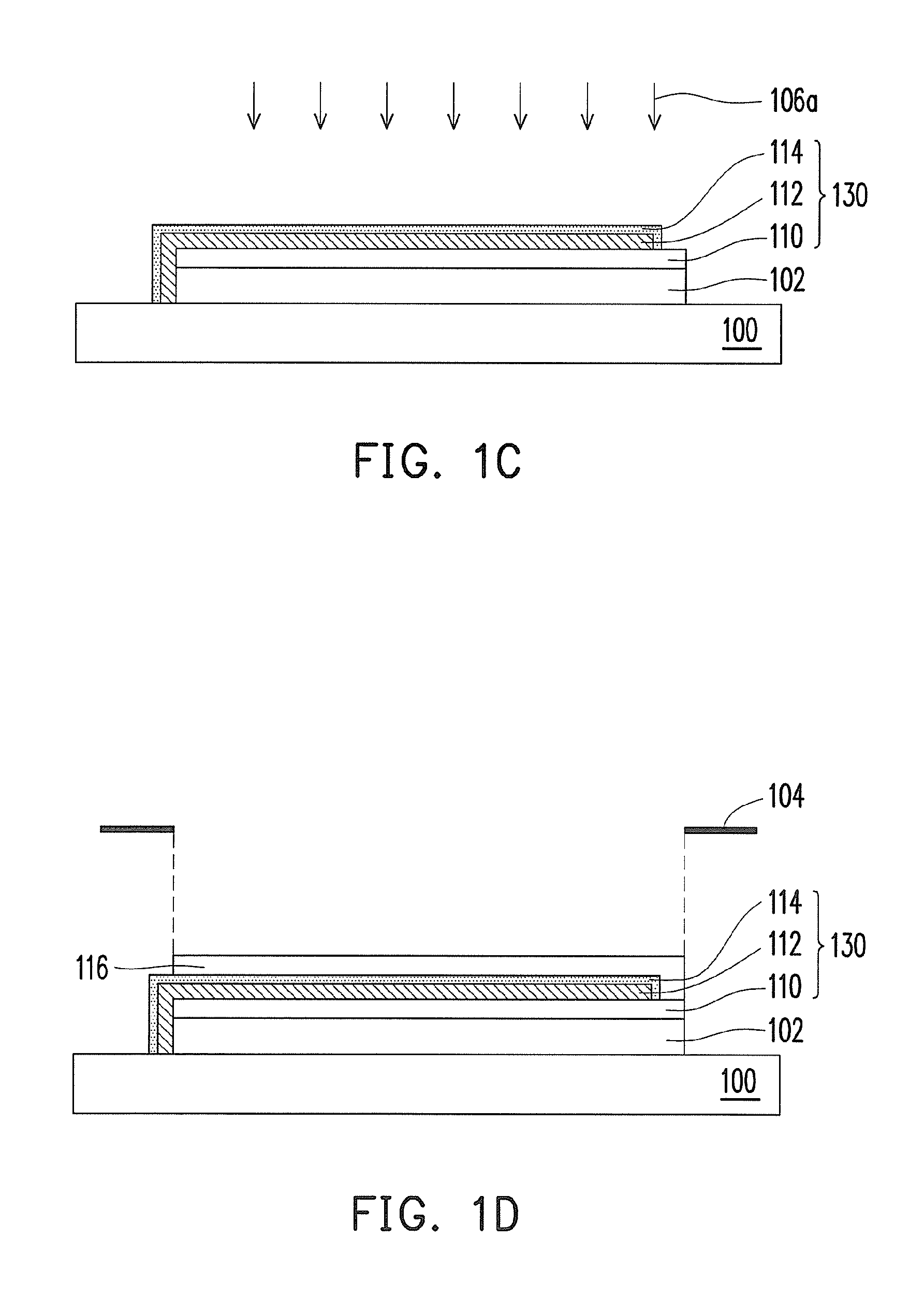
Apparatus of organic light emitting diode and packaging method of the same
a technology of organic light-emitting diodes and packaging methods, which is applied in the manufacture of electrode systems, discharge tubes luminescnet screens, electric discharge tubes/lamps, etc., can solve the problems of reducing unable to ensure that the oled is not affected by water vapor and oxygen, and no space for the getter present, etc., to achieve the effect of increasing the life of the devi
- Summary
- Abstract
- Description
- Claims
- Application Information
AI Technical Summary
Benefits of technology
Problems solved by technology
Method used
Image

Examples
example 1
[0063]FIG. 4A schematically illustrates a cross-sectional view of a stacked structure according to Example 1 of the present invention.
[0064]Referring to FIG. 4A, a polyimide (PI) substrate 400a was provided, and an organic layer 402a and a metal layer 404a were sequentially formed on the substrate 400a. The material of the organic layer 402a was pentacene, and the thickness of the same was about 150 nm. The material of the metal layer 404a was aluminum and the thickness of the same was about 150 nm. Thereafter, the WVTR of the stacked structure was measured by MOCON Permatran W3 / 60 Water Vapor Permeability and the temperature of the substrate 400a was measured at the same time.
example 2
[0065]FIG. 4B schematically illustrates a cross-sectional view of a stacked structure according to Example 2 of the present invention.
[0066]Referring to FIG. 4B, a UV ozone process 408b was performed to a stacked structure obtained in Example 1, so as to form a metal oxide layer 406a on the surface of the metal layer 404b. During the step of performing the UV ozone process 408b, the gas source was selected from the group consisting of ozone, oxygen and nitrogen, and the process time was about 5 minutes. Thereafter, the testing of the stacked structure in Example 2 was done by following the measurement step described in Example 1.
example 3
[0067]FIG. 4C schematically illustrates a cross-sectional view of a stacked structure according to Example 3 of the present invention.
[0068]Referring to FIG. 4C, a UV ozone process 408c was performed to a stacked structure obtained in Example 1, so as to form a metal oxide layer 406c on the surface of the metal layer 404c. During the step of performing the UV ozone process 408c, the gas source was selected from the group consisting of ozone, oxygen and nitrogen, and the process time was about 15 minutes. Thereafter, the testing of the stacked structure in Example 3 was done by following the measurement step described in Example 1.
PUM
 Abstract
Description
Claims
Application Information
 - R&D
- Intellectual Property
- Life Sciences
- Materials
- Tech Scout
- Unparalleled Data Quality
- Higher Quality Content
- 60% Fewer Hallucinations
Browse by: Latest US Patents, China's latest patents, Technical Efficacy Thesaurus, Application Domain, Technology Topic, Popular Technical Reports.
© 2025 PatSnap. All rights reserved.Legal|Privacy policy|Modern Slavery Act Transparency Statement|Sitemap|About US| Contact US: help@patsnap.com